Explaining Common Chip Terms

You know what a semiconductor is, but what’s a die? Wafer? Substrate? Learn the basics of all things chips.

Like most sectors of science and technology, the world of semiconductors has its own esoteric language, acronyms and initialisms (Oh, the three-letter acronyms as TLAs!).
Your friends at Intel are here to help.
This edition of Tech 101 aims to define the most common terms used in chipmaking, from chip itself to PDKs and PPA.
Wafers Become Dies, Packaging Makes Chips
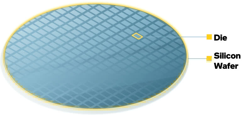
A wafer is a circular slice of ultra-pure silicon (a natural semiconductor, remember?). Intel uses modern wafers that are 300 millimeters (12 inches) in diameter and only 0.775 mm thick – about the same as a credit card. Silicon purity ranges from 99.9999% to 99.9999999% – denoted as 6N to 9N purity, respectively.
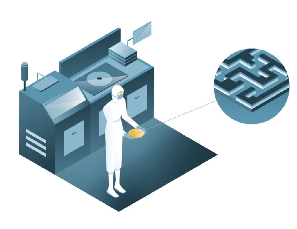
During fabrication, multiple identical integrated circuits are created on a single large wafer. The wafer is then sliced – or diced – into pieces, each called a die.
To become usable, dies are packaged – alone or with other dies – into a form that can be installed in a computer or smart device.
The definition of chip is less rigid — while it can refer to a single die (which is like a little chip of glass), usually it’s associated with the packaged version since that’s the only way the non-chipmaking public encounters it.
Wouldn’t Square Wafers be Better?
You might guess so since dies are rectangular, but no.
Silicon wafers are round because they start as cylindrical ingots, grown by rotating a seed crystal in molten silicon.
This round shape is easy to slice, handle and process, ensuring stability during manufacturing. Circular wafers also minimize material waste and reduce the risk of chipping.
Adjacent thought experiment: Why aren’t pizza boxes round?
Process Nodes and PDKs
The recipe and list of ingredients used in semiconductor fabrication is called a process node. A node specifies the physical architecture of the components – most notably the transistors and the wiring that connects them, called interconnects – and the thousands of steps to build them.
The characteristics that separate nodes include transistor size and density, power efficiency, performance, cost, thermal management, and accompanying features. If we get things right, Moore’s Law progresses forward with each new node.
In the past, process node names were based on physical measurements in micrometers or nanometers (like 0.13 microns or 45 nanometers), but current names are closer to representations of each node’s increase in density and/or performance. Recent Intel process nodes include Intel 7, Intel 3 and Intel 18A, which establishes the Angstrom Era of chipmaking.
A process design kit, or PDK, is a set of specifications, guidelines and tools to design a chip using a specific process node. A PDK is like a recipe, giving designers a set of ingredients and rules on how to combine them.
What is a Package?
The Tech 101 on assembly and test illustrates how dies get dressed for work. In short, dies are mounted to a package, which provides protection from heat and outside elements, physical strength, and connections to the computer.
The material that dies are attached to and that provides the foundation of the package is called the substrate. It is composed of materials like organic laminates, ceramics or glass.
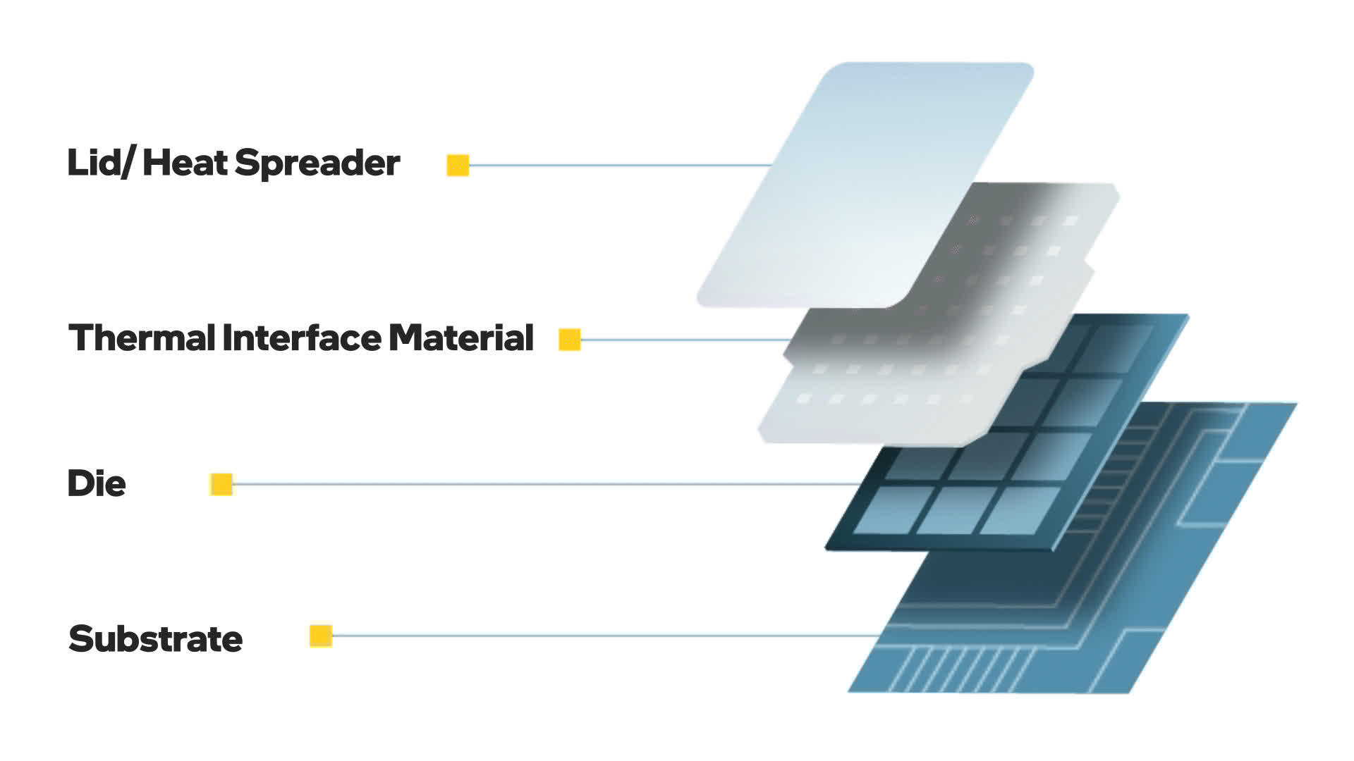
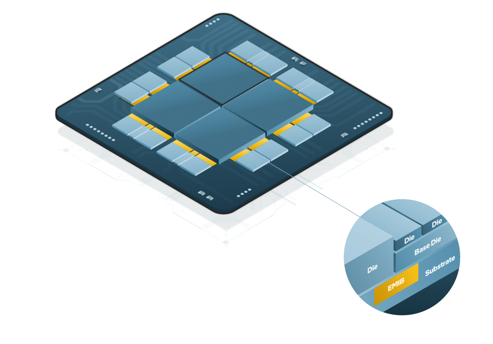
In the past, most packages contained a single die. Advanced packaging refers to a set of specialized technologies introduced over the past decade to combine multiple dies in a single package. Dies can be stacked or closely connected in ways that mimic a single die – packing more functionality and computing capability into one device.
Examples of Intel’s advanced packaging are:
EMIB (embedded multi-die interconnect bridge), which allows chips to be connected side by side and
Foveros to stack chips on top of another.
Small companion dies connected with advanced packaging are often referred to as chiplets.
Measuring Process Nodes with Yield and PPA
Yield refers to the percentage of usable die that are produced on a processed wafer. The yield will vary depending on the size of each die and the defect density, or the number of defects in the silicon per area. Ideally, a low defect density leads to higher yields.
Each chip’s design will dictate die size (more functionality requires more area). A denser process node will result in smaller die. Given the same defect density, a smaller die will produce a higher yield than a larger die.
Process nodes are compared and evaluated with three primary metrics: power, performance and area – known collectively as PPA. The goal is always to lower power consumption, increase performance and minimize silicon real estate area — all at the lowest possible cost.
The rise of advanced packaging and multi-chip devices that combine many dies together, however, makes considerations like heat and power management more complex. Compromise abounds.

Summary
- Silicon dies are built on and sliced from circular wafers, and then packaged with substrates to create computer chips.
- Process nodes detail the ingredients and recipe used to build silicon dies. Chip architects use process design kits to design chips on a specific node.
- Semiconductor engineers work relentlessly to raise performance and quality, lower power consumption and cost and shrink everything.
- Download this Tech 101
Ready to discover more?
The Intel Tech 101 series mixes visuals and descriptions to break down complex subjects and demystify the technology we use every day.