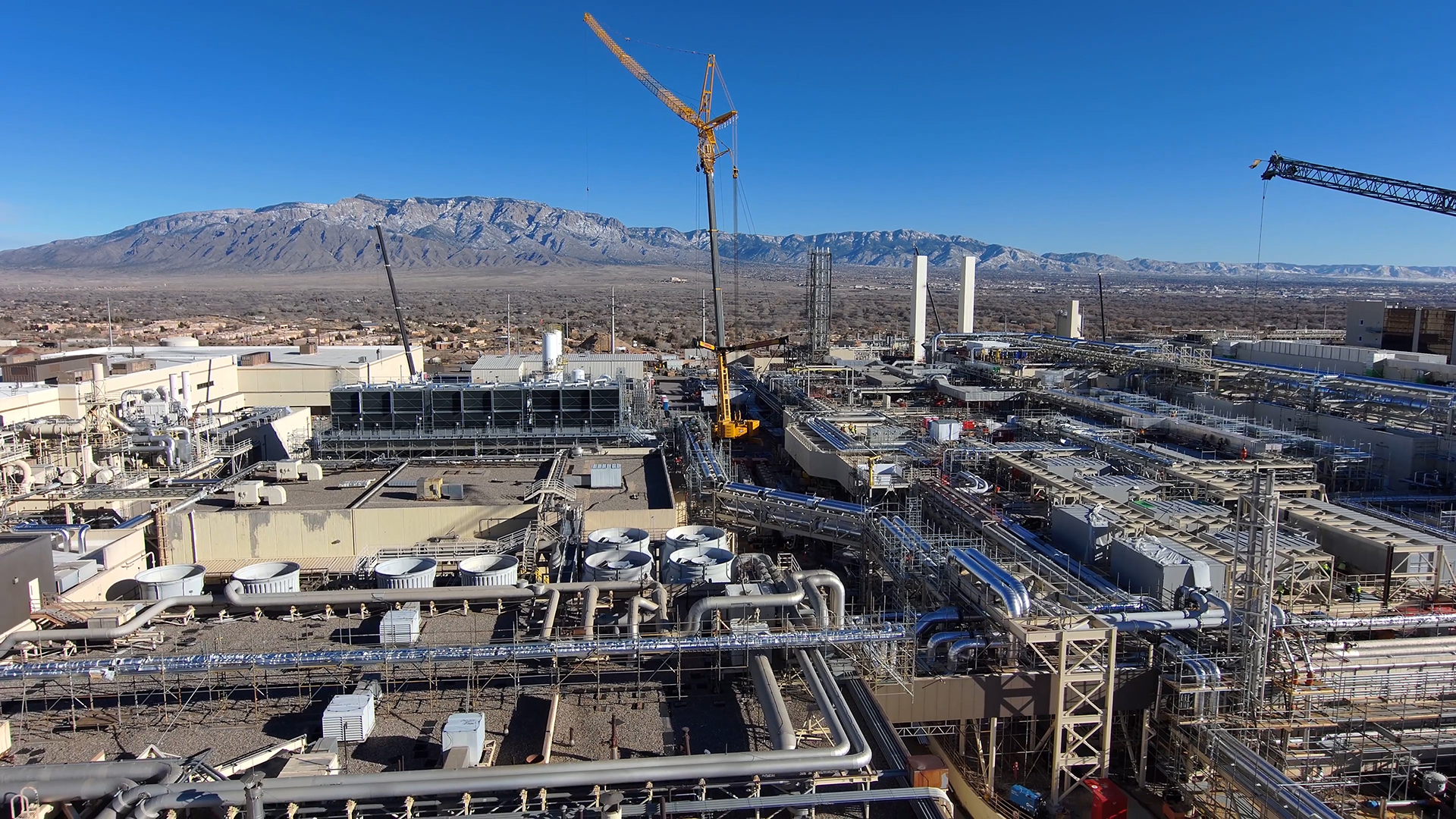
Listen to audio
Loading...
Play
Pause
1x
Playback Speed- 0.5
- 0.6
- 0.7
- 0.8
- 0.9
- 1
- 1.1
- 1.2
- 1.3
- 1.5
- 2
英特尔实现3d先进封装技术的大规模量产. january 24, 2024 发布 英特尔代工 a drone photo shows intel's new fab 9 in rio rancho, new mexico, in january 2024. fab 9 is part of intel's previously announced $3.5 billion investment to equip its new mexico operations for the manufacturing of advanced semiconductor packaging technologies. (credit: intel corporation). 在本文中: 
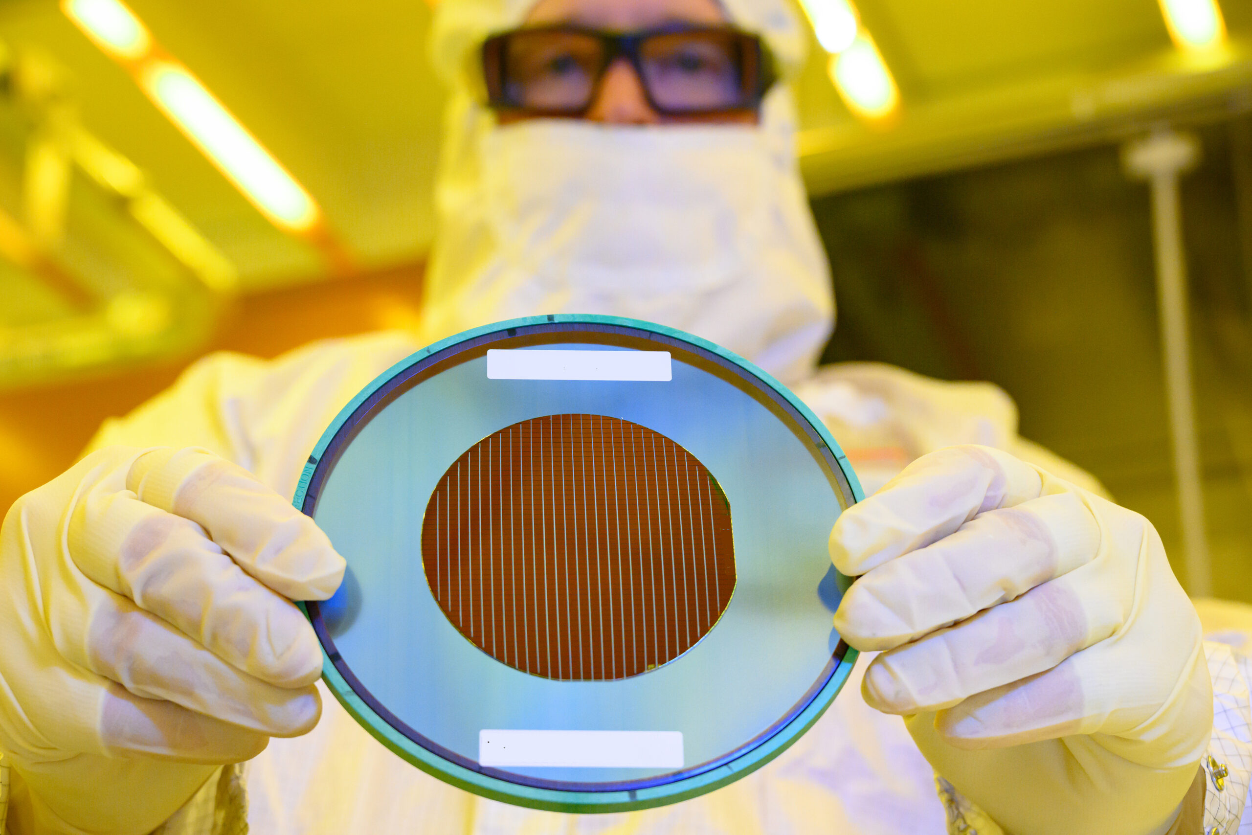
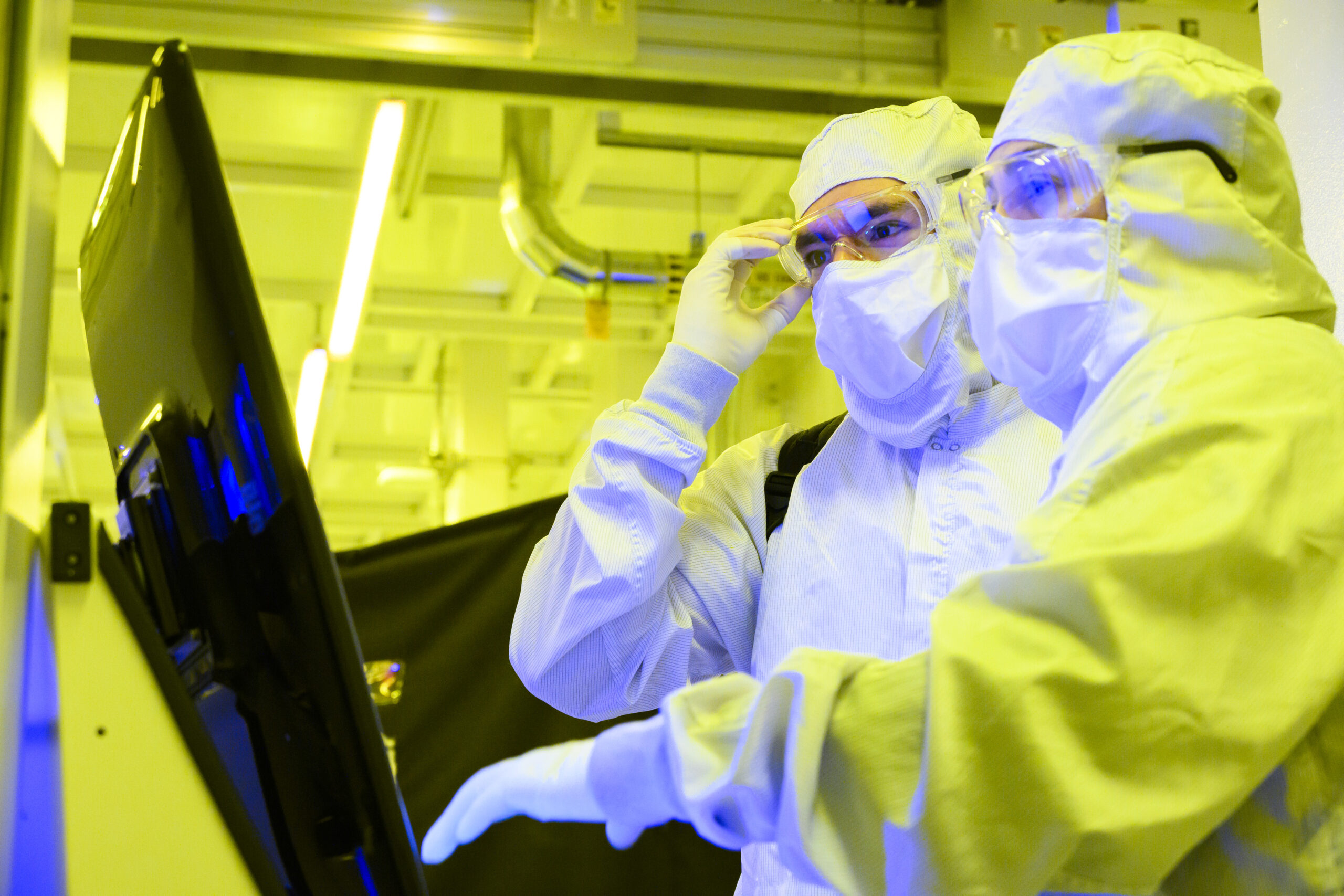
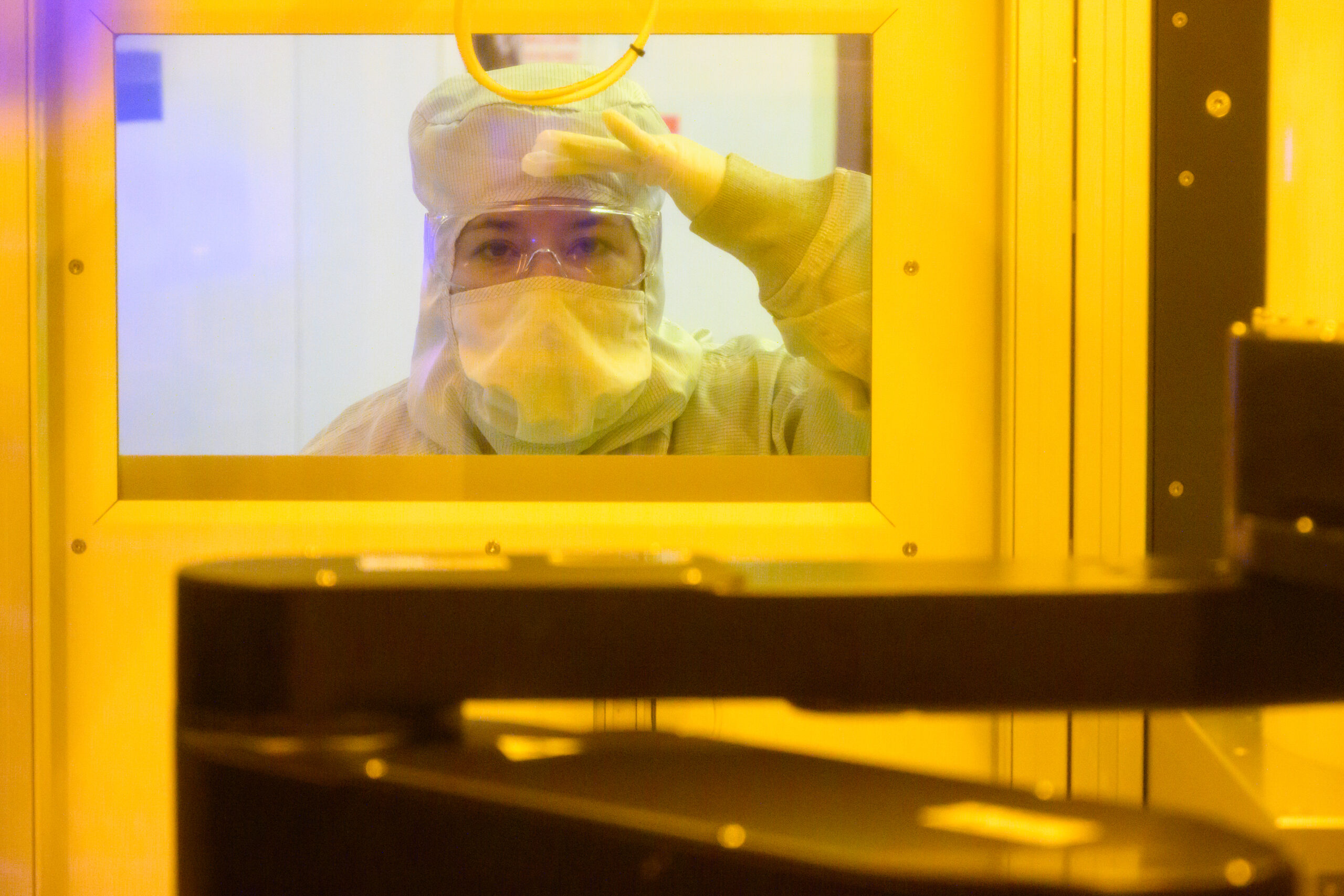
英特尔宣布已实现基于业界领先的半导体封装解决方案的大规模生产,其中包括英特尔突破性的3d封装技术foveros,该技术为多种芯片的组合提供了灵活的选择,带来更佳的功耗、性能和成本优化。. 这一技术是在英特尔最新完成升级的美国新墨西哥州fab 9投产的。. 先进封装技术让英特尔脱颖而出,帮助我们的客户在芯片产品的性能、尺寸,以及设计应用的灵活性方面获得竞争优势。. —keyvan esfarjani 英特尔公司执行副总裁 兼首席全球运营官 这一里程碑式的进展还将推动英特尔下一阶段的先进封装技术创新。随着整个半导体行业进入在单个封装中集成多个“芯粒”(chiplets)的异构时代,英特尔的foveros和emib(嵌入式多芯片互连桥接)等先进封装技术提供了速度更快、成本更低的路径,以实现在单个封装中集成一万亿个晶体管,并在2030年后继续推进摩尔定律。
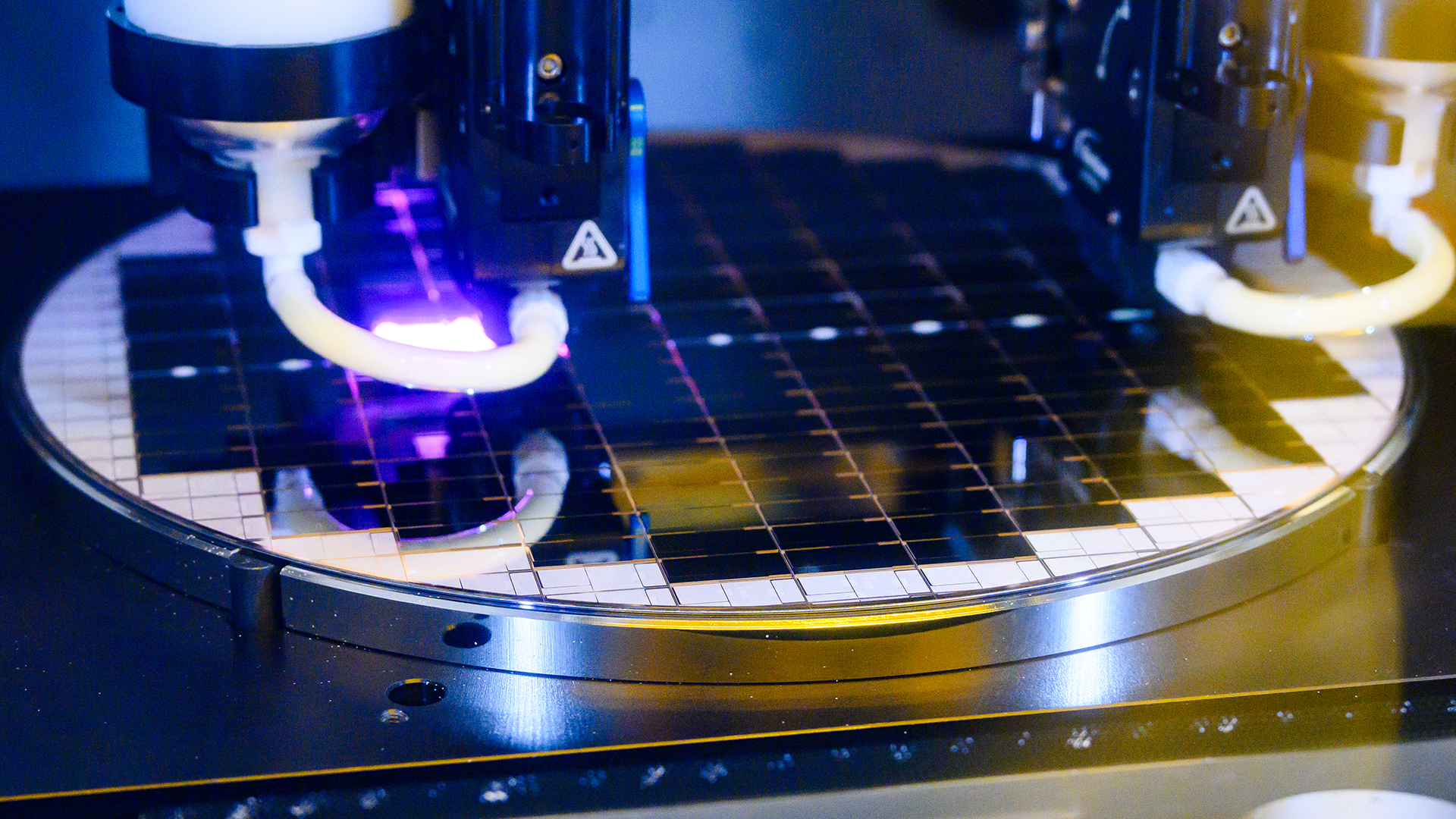
. 英特尔的3d先进封装技术foveros是业界领先的解决方案,在处理器的制造过程中,能够以垂直而非水平方式堆叠计算模块。此外,foveros让英特尔及其代工客户能够集成不同的计算芯片,优化成本和能效。. 英特尔将继续致力于推进技术创新,扩大业务规模,满足不断增长的半导体需求。. a drone photo shows intel's new fab 9 in rio rancho, new mexico, in january 2024. fab 9 is part of intel's previously announced $3.5 billion investment to equip its new mexico operations for the manufacturing of advanced semiconductor packaging technologies. (credit: intel corporation). keyvan esfarjani (center), intel chief global operations officer, cuts the ribbon in the ceremonial opening of fab 9 in rio rancho, new mexico, on wednesday, jan. 24, 2024. he is joined at an employee celebration with local elected officials and intel managers (from left): rio rancho mayor greggory hull; ali diouf, fab 9 factory manager; u.s. rep. teresa leger fernández; sandoval county commission chairman david heil; u.s. rep. melanie stansbury; new mexico gov. michelle lujan grisham; esfarjani; katie prouty, intel new mexico plant manager; peter charvat, general manager of disaggregation manufacturing organization; brian chavez, f11x factory manager; mindy koch, new mexico corporate services site manager; and kenneth nava, new mexico director of fab construction enterprise. (credit: intel corporation). manufacturing technicians work in the clean room of intel's new fab 9 in rio rancho, new mexico, in january 2024. (credit: intel corporation). a manufacturing technician looks through a window of advanced packaging equipment at intel's new fab 9 in rio rancho, new mexico, in january 2024. (credit: intel corporation). a photo from january 2024 at intel's new fab 9 in rio rancho, new mexico shows chiplet bonding as part of intel's advanced packaging technology called foveros. this breakthrough 3d packaging technology offers flexible options for combining multiple chips that are optimized for power, performance and cost. (credit: intel corporation). a wafer moves through the manufacturing process at intel's new fab 9 in rio rancho, new mexico, in january 2024. (credit: intel corporation). an intel manufacturing technician at fab 11x in rio rancho, new mexico, holds a bond module carrier containing a single silicon photonics chip in january 2024. these intel products enable future data center bandwidth growth and next-generation 5g deployments using smaller form factors and higher speeds. (credit: intel corporation). 下载所有图像 (zip, 81 mb)下载视频:“ 英特尔在新墨西哥州 9 号工厂的先进封装,11x 制造 (b-roll)” “ 英特尔在新墨西哥州 9 号工厂的先进封装,11x 制造 (b-roll)”. intel advanced packaging in new mexico’s fab 9, manufacturing in fab 11x (b-roll).