Meet the Intel Pioneer Behind EMIB Chip Packaging
Ravi Mahajan discusses the idea for a simple silicon bridge and why it is becoming a foundational technology for the AI era.
Ravi Mahajan is a foundational figure behind Intel’s leadership in advanced packaging. As an Intel Fellow and director of Substrate and Advanced Packaging Pathfinding at Intel Foundry, he has spent more than 30 years advancing semiconductor packaging technologies.
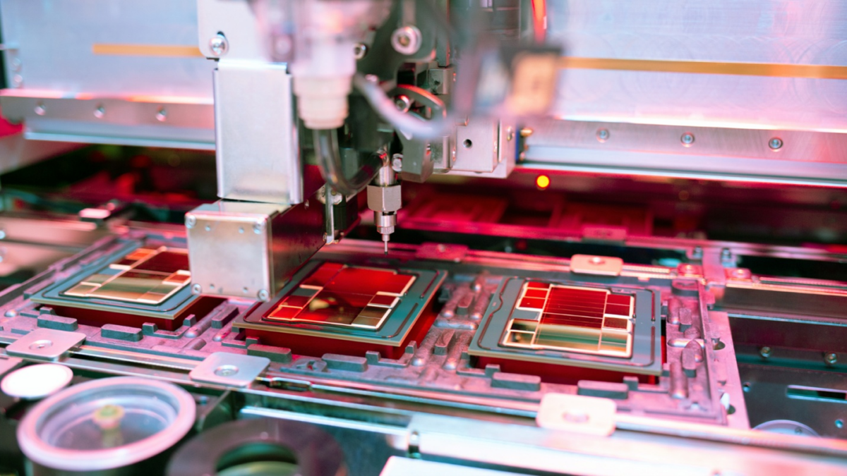
Often referred to as the inventor of EMIB (Embedded Multi-die Interconnect Bridge), Mahajan led the development of this groundbreaking technology that enables multiple chips to be tightly interconnected within a single package, an increasingly important capability as AI workloads drive demand for higher performance, bandwidth and energy efficiency.
In this conversation, he reflects on his career, the origins of EMIB, the growing importance of advanced packaging, and why system-level innovation is becoming central to the future of computing.
Q: Why is advanced packaging increasingly at the center of global technology conversation?
For decades, the semiconductor industry relied on transistor scaling—what we often refer to as Moore’s Law—to drive performance improvements. 
At the same time, demand for compute has accelerated dramatically, especially with AI. These workloads require not just more compute, but significantly higher memory bandwidth, and energy efficiency especially in managing the data traffic.
Advanced packaging has emerged as a critical new lever. It allows us to bring multiple chips together in a highly integrated way, enabling system-level performance gains that would not be possible through monolithic scaling alone.
Q: You’ve spent more than three decades at Intel. What changes have you seen in how the industry approaches packaging?
When I joined Intel more than 30 years ago, packaging was often viewed as a supporting function: important, but not a primary driver of performance.
That has completely changed. Today, packaging is central to system design. We are no longer just protecting silicon, we are enabling new architectures by determining how different components connect, communicate, and perform together.
The scale of change is remarkable. Early in my career, we were concerned about cooling a few watts of power. Today, we are managing systems at kilowatt levels. That shift reflects how much more important system-level optimization has become.
Q: You are often described as the father of EMIB. How did EMIB originate?
In the early 2000s, we began asking whether packaging had its own version of a scaling roadmap. One key limitation we identified was interconnect density—how many signals you can efficiently route in and out of a chip.
Traditional approaches were not scaling fast enough to meet future needs. That led us to explore whether we could introduce silicon-based interconnects directly into the package to dramatically increase density.
The concept behind EMIB was to use a small piece of silicon embedded in the package to connect chips at a very fine pitch. It was a simple idea conceptually, but it required solving complex challenges in materials, stress management, and manufacturing.
By 2013, we were confident enough to bring EMIB into a production program and then introduced it to the public the following year. It has since become a foundational technology for high-performance systems.
The key insight was this: if you can’t scale everything on one chip, you can scale the system by connecting multiple optimized chips together—and do so in a way that preserves performance and efficiency.
Q: How does advanced packaging impact the performance and scalability of AI systems?
AI systems are fundamentally constrained by how quickly data can move between compute and memory. As models grow larger and more complex, that data movement becomes the limiting factor.
Advanced packaging directly addresses this challenge. By enabling high-density, energy-efficient connections between compute, memory, and switches, we can significantly increase bandwidth while reducing power consumption.
This is essential for scaling AI. Without innovations in packaging, it would be much harder to deliver the performance improvements that modern AI workloads require.
Q: What does EMIB and advanced packaging enable for Intel Foundry customers?
It gives customers much more flexibility in how they design their systems.
Instead of building a single, very large chip, they can combine multiple smaller chips—each optimized for a specific function—into one integrated package. That can improve performance, overcome reticle limits, reduce cost, and accelerate time to market.
It also allows customers to mix and match technologies, including different process nodes or even different vendors, depending on what best meets their needs.
From a foundry perspective, this is immensely powerful. We are enabling customers to design at the system level, not just the chip level.
Q: What differentiates Intel’s approach to advanced packaging?
One key advantage is that we can take innovations from research to high-volume manufacturing.
Advanced packaging is about execution at scale. You need infrastructure, process technology, and engineering depth to make these solutions manufacturable and reliable.
We also benefit from strong integration across disciplines, including design, materials science, process engineering, and manufacturing. That allows us to optimize the entire system, not just individual components.
Q: What are the biggest challenges as packaging becomes more complex?
As we push toward higher interconnect density, we also increase complexity across materials, assembly, and system integration.
We need to ensure reliability across many different components, manage thermal performance at very high-power levels, and maintain strong manufacturing yields as designs become more intricate.
Power delivery is another major challenge. As systems scale, delivering power efficiently becomes just as important as moving data efficiently.
Addressing these challenges requires deep expertise across multiple disciplines, along with advanced modeling, testing, and manufacturing capabilities.
Q: What needs to happen across the industry to accelerate progress in advanced packaging?
Collaboration is essential. The challenges we are solving are too complex for any one company to address alone.
We need alignment across the ecosystem, from materials and equipment to design and standards. Historically, industry roadmaps helped guide progress. There is an opportunity to strengthen that kind of coordination again, especially as packaging becomes more central to system performance.
Q: Looking ahead, what future technologies will define leadership in advanced packaging over the decade?
Interconnect scaling will remain a key focus, both electrically and optically. We are already exploring new approaches, including co-packaged optics, to further increase bandwidth and efficiency.
New materials, such as glass substrates, also have significant potential to improve performance and scalability.
Leadership will come down to the ability to integrate complex systems efficiently and reliably at scale. The companies that can do that—while continuing to innovate—will define the future of computing.
Q: Why are you optimistic about Intel’s ability to lead in advanced packaging?
Intel has a long history of innovation and a strong track record of bringing complex technologies to market.
We have deep engineering expertise, advanced infrastructure, and a culture of collaboration across disciplines. Just as importantly, we are investing in the next generation of talent and capabilities needed to continue advancing the field.
All that gives me confidence that we can help shape the future of advanced packaging and the broader semiconductor industry.
Related Posts
 Intel Foundry
Intel Completes RAMP-C Program, Accelerating Momentum for Secure Enclave
Program enabled validated prototypes, ecosystem readiness, and early customer engagement, creating a path to domestic leadership in high-volume manufacturing
July 28, 2026
New Technologies
Intel and Lens Technology Collaborate to Enable Advanced Semiconductor Packaging for the AI Era
Collaboration combines Intel's advanced packaging expertise with Lens Technology's precision glass processing capabilities to deliver enhanced performance for future AI and datacenter workloads
July 24, 2026