Press Kit: Global Manufacturing at Intel
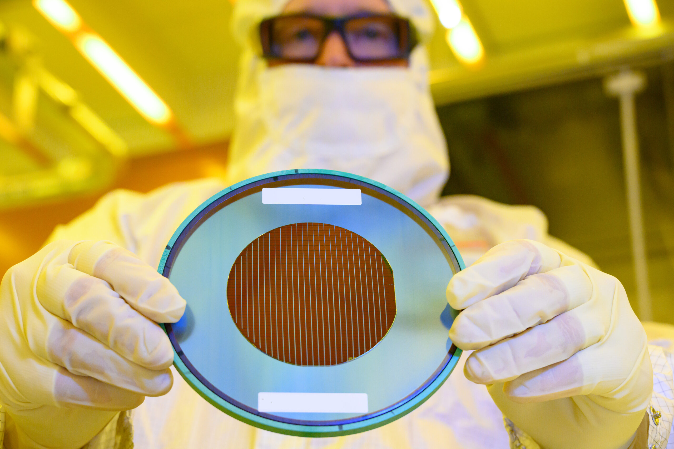
Production and cleanroom facilities at work in Intel’s D1D/D1X plant in Hillsboro, Oregon, in April 2017. (Credit: Intel Corporation)
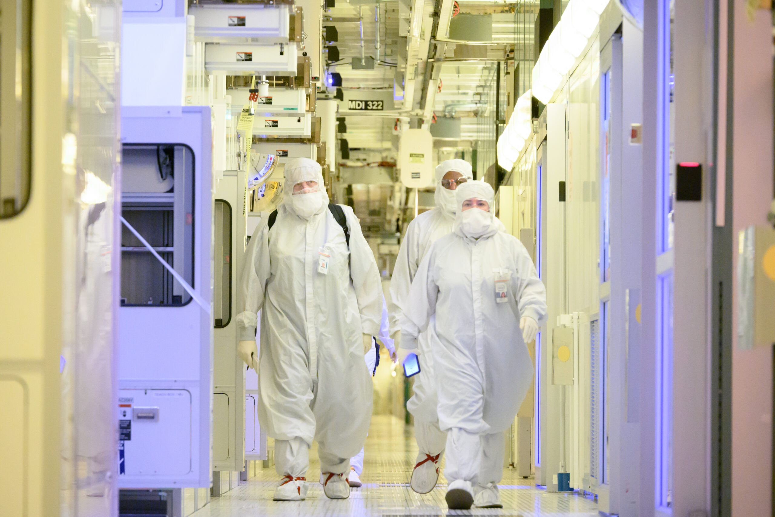
Intel manufacturing operates at a mega-scale worldwide.
Squeezing billions of tiny transistors onto ever-smaller computer chips requires one of the most complex manufacturing processes humans have devised. A fully equipped new fab costs about $10 billion and takes 6,000 construction workers about three years to complete. Intel’s manufacturing operations operate at a mega-scale worldwide, requiring a global supply chain that stretches across multiple continents.
News
- New Mexico, USA: Intel Opens Fab 9 in New Mexico
- Oregon, USA: Intel's Oregon Investments Fuel US Silicon Innovation Leadership
- Ireland: Intel’s New Fab in Ireland Begins High-Volume Production of Intel 4 Technology
- Poland: Intel Plans Assembly and Test Facility in Poland
- Ohio, USA: Intel Announces Next US Site with Landmark Investment in Ohio | Intel Invests in Ohio (Press Kit)
- Ireland: Ireland Milestone: First Tool Roll-in at Fab 34
- Worldwide: All Intel Manufacturing News
- United States: Competitiveness is at Stake for Chip Manufacturing (Bruce Andrews Editorial)
- Worldwide: Intel CEO Pat Gelsinger Announces ‘IDM 2.0’ Strategy for Manufacturing, Innovation and Product Leadership
- Arizona, USA: Intel Breaks Ground on Two New Leading Edge Chip Factories in Arizona
- New Mexico, USA: Intel Invests $3.5 Billion in New Mexico Operations (Press Kit)
Global Investments
Infographic: Global Investments Announced Since 2021
Download full size infographic
B-roll Video
» All Intel Manufacturing, Office and Construction B-Roll Videos
Manufacturing in Vietnam
Intel Manufacturing in Vietnam (B-Roll)
B-roll video footage shows the Vietnam Assembly Test (VNAT) facility in April 2023. (Credit: Intel Corporation)
Download "Intel Manufacturing in Vietnam (B-Roll)"
Manufacturing in Malaysia
Intel Manufacturing in Penang, Malaysia (B-Roll)
Video footage from April 2023 shows the Intel Penang Assembly Test (PGAT) facility in Penang, Malaysia. It includes Intel employees inside the facility and video of Intel Core Ultra processors, code-named Meteor Lake. (Credit: Intel Corporation)
Download video: "Intel Manufacturing in Penang, Malaysia (B-Roll)"
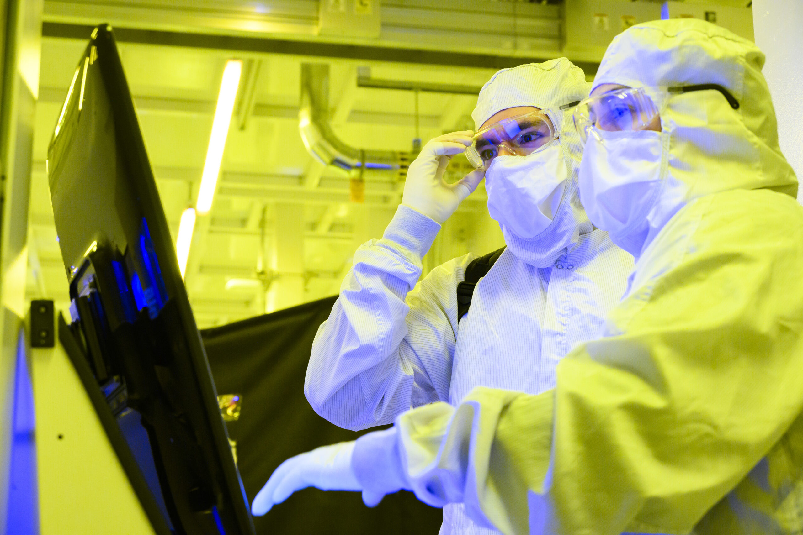
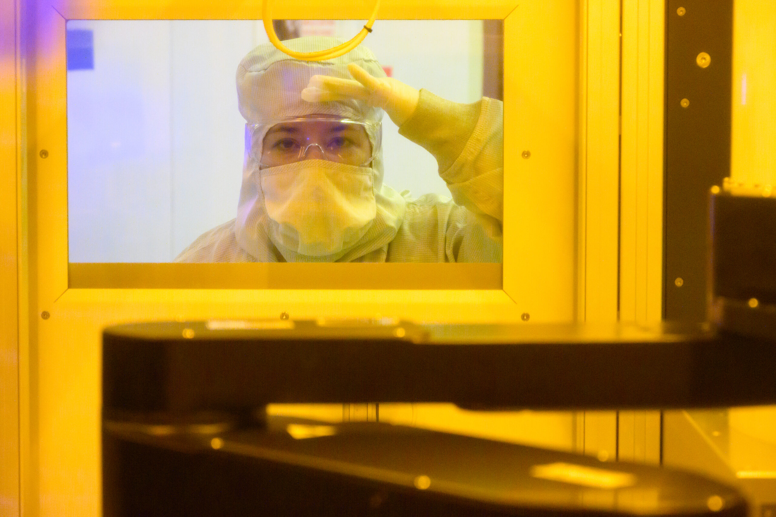
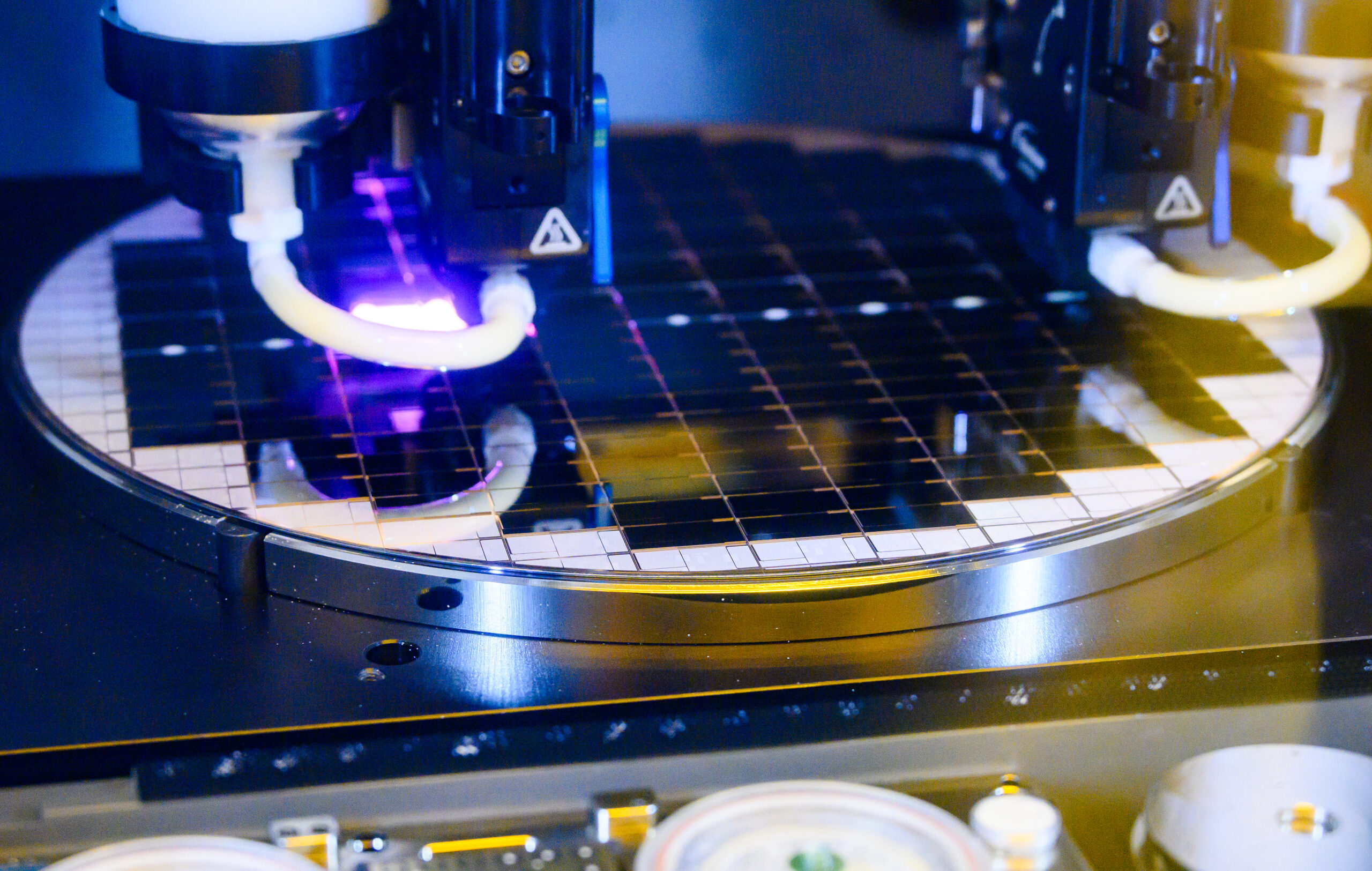
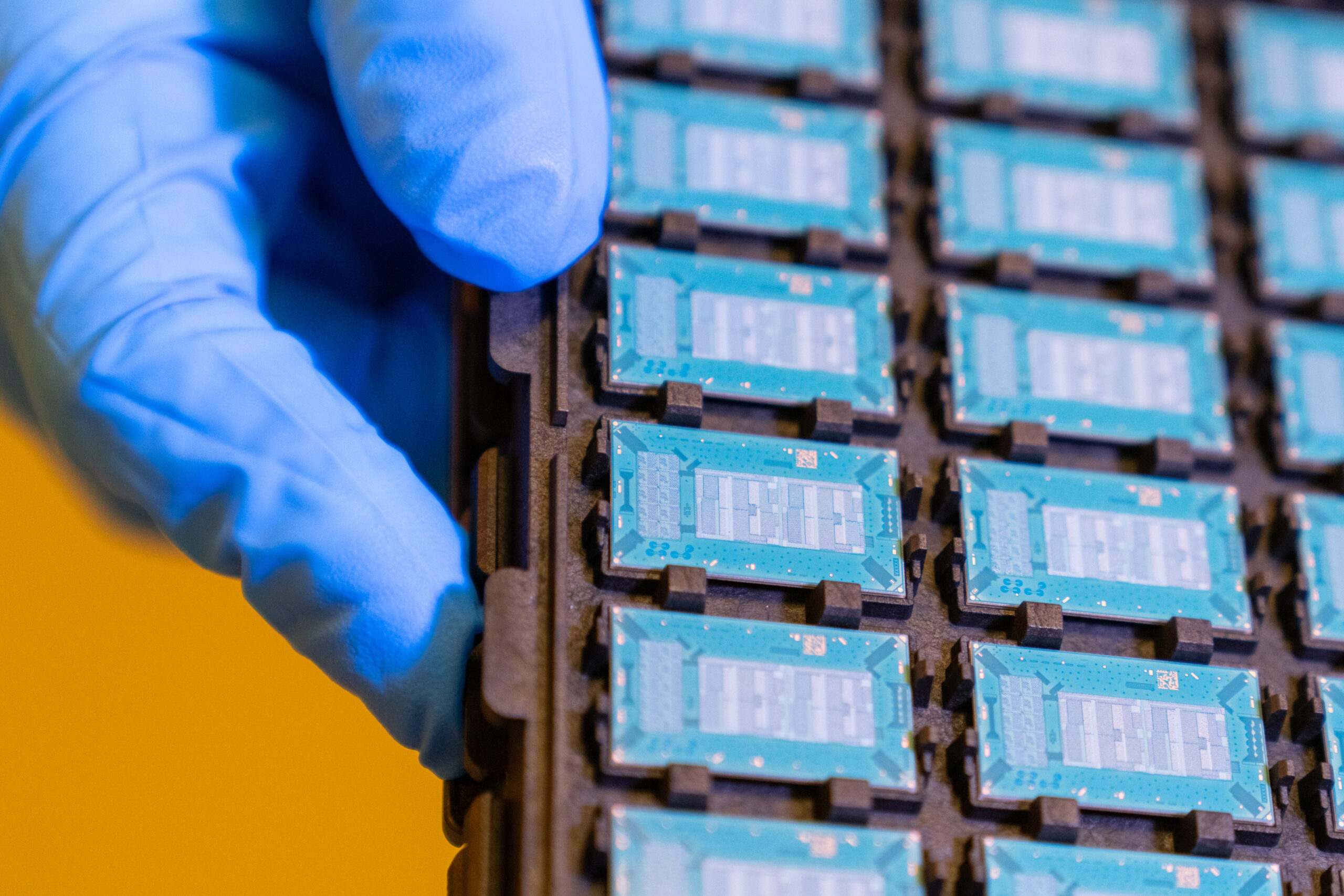
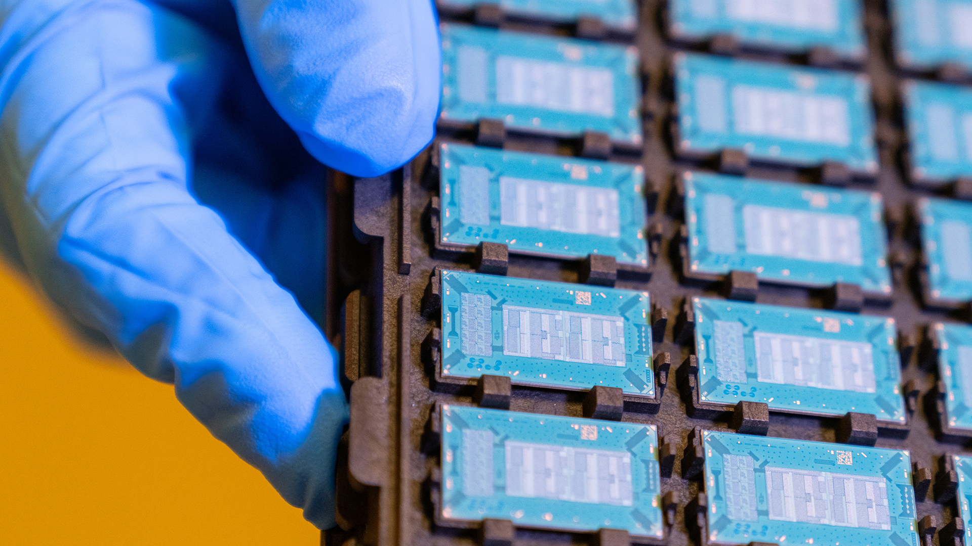
Manufacturing in Oregon, USA


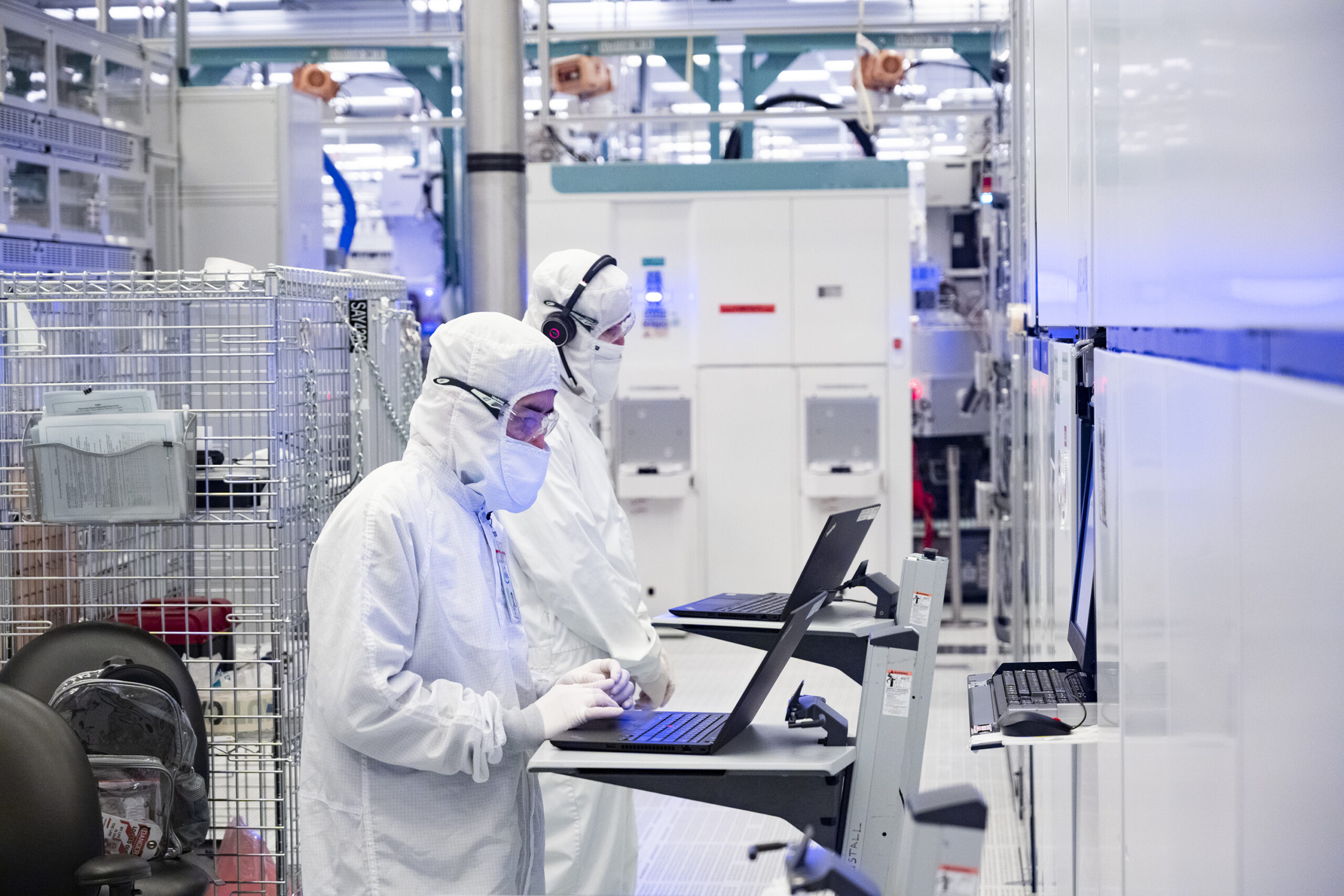
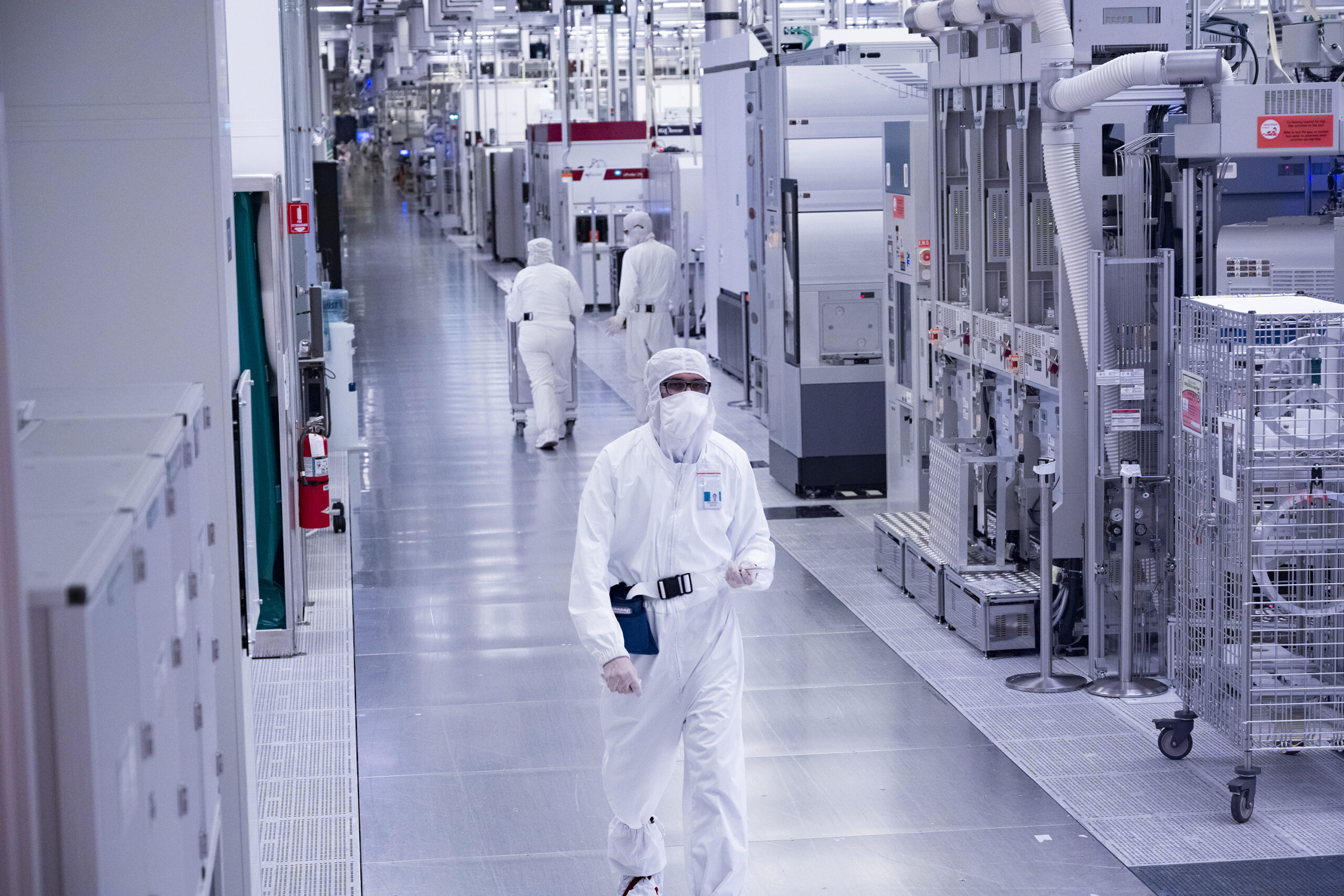
» Download all images (ZIP, 37 MB)

Manufacturing Infographic
Automated Material-Handling System
Travel Intel’s Autonomous Superhighway
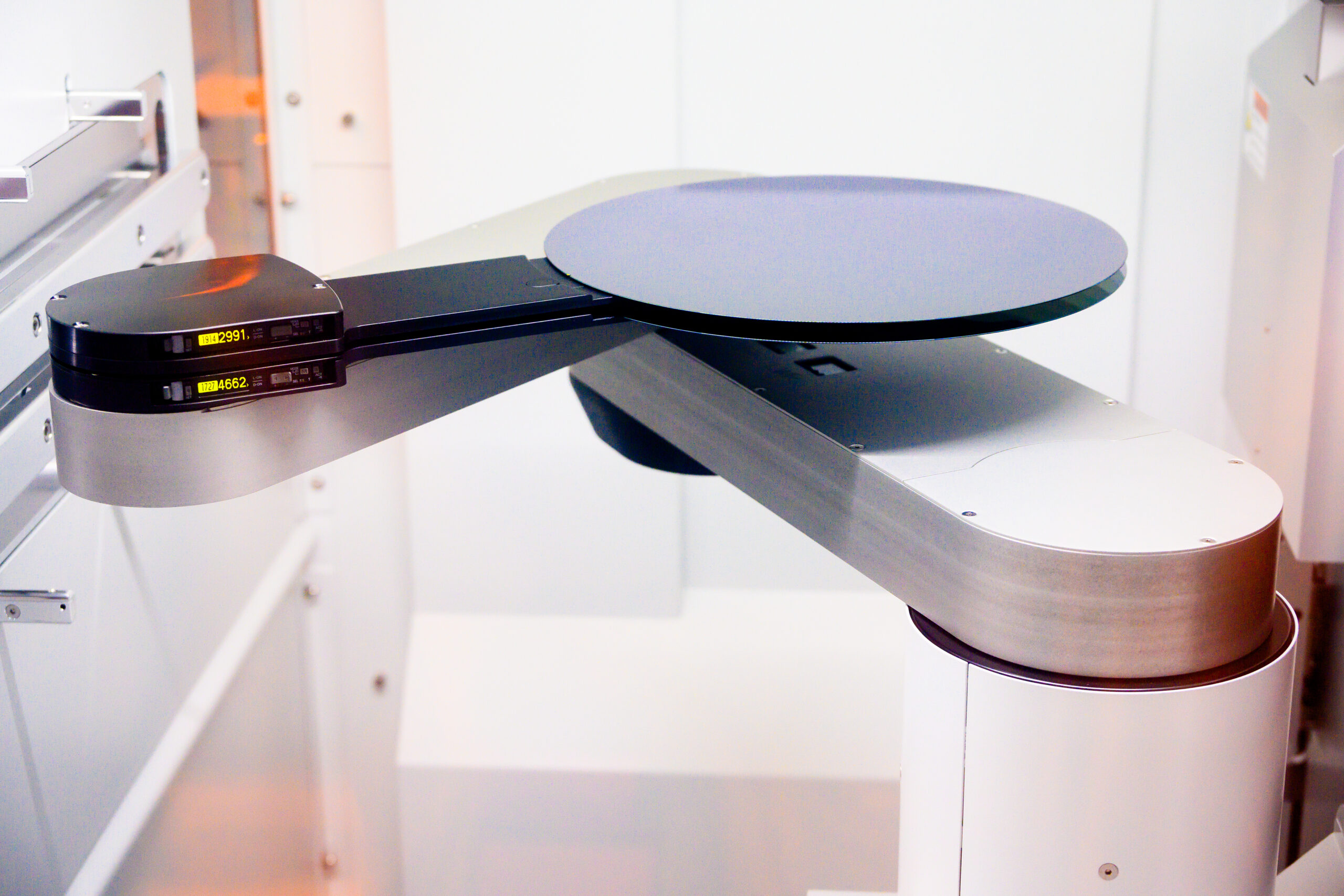
It has more than 27 miles of multilevel thoroughfares on which 1,700 autonomous vehicles shuttle Intel’s most precious cargo. It’s the automated material-handling system – or AMHS – at Intel’s D1 factory in Hillsboro, Oregon. Intel runs overhead transport systems like this in every one of its six chip fabs worldwide. The boxes scooting along on the overhead tracks are front-opening unified pods – or FOUPs – that carry as many as 25 wafers, each containing hundreds of Intel® chips, on their weekslong fabrication journey starting as blank silicon discs.
Oregon’s wafer superhighway connects nine buildings, including the D1X and D1D factories. The two factories together are a little larger than 12 U.S. football fields. Take a quick 2-minute tour around Oregon’s D1 factory — captured before pandemic recommendations for social distancing took effect — to learn more about what AMHS leader Mutaz Haddadin calls the “heartbeat and blood flow of the fab.”
» View video: Intel’s Automated Superhighway: ‘The Heartbeat and Blood Flow of the Fab’
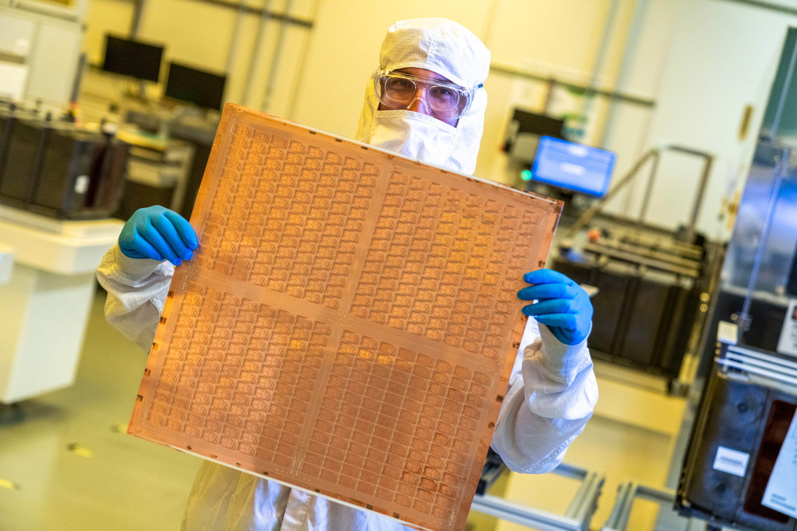
Manufacturing in New Mexico, USA
Intel Advanced Packaging in New Mexico’s Fab 9, Manufacturing in Fab 11X (B-Roll)
Download video: "Intel Advanced Packaging in New Mexico’s Fab 9, Manufacturing in Fab 11X (B-Roll)"


Download all images (ZIP, 89 MB)
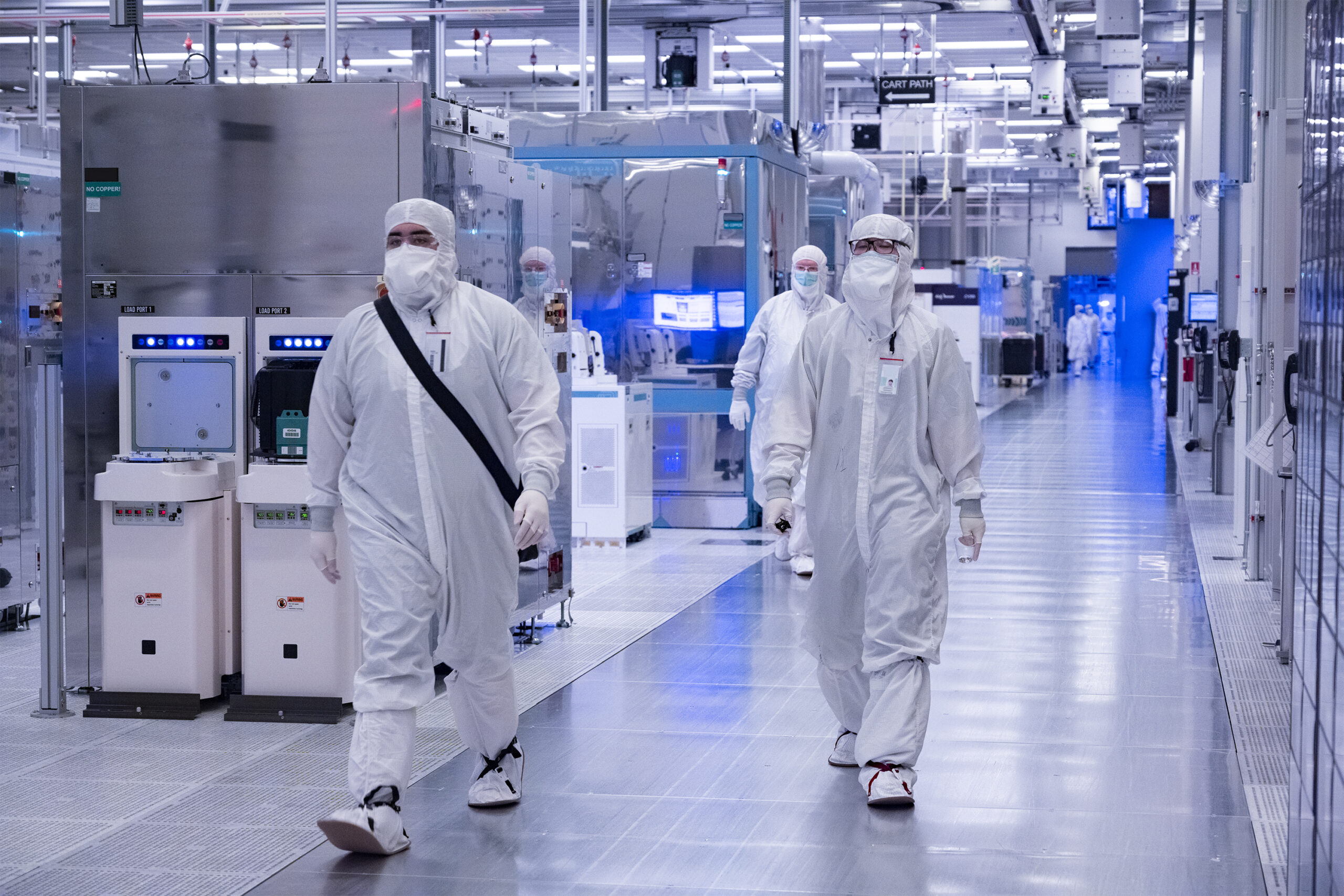
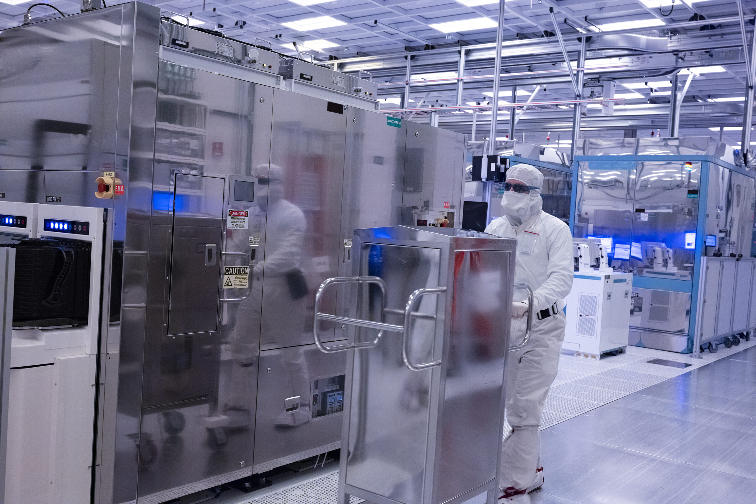
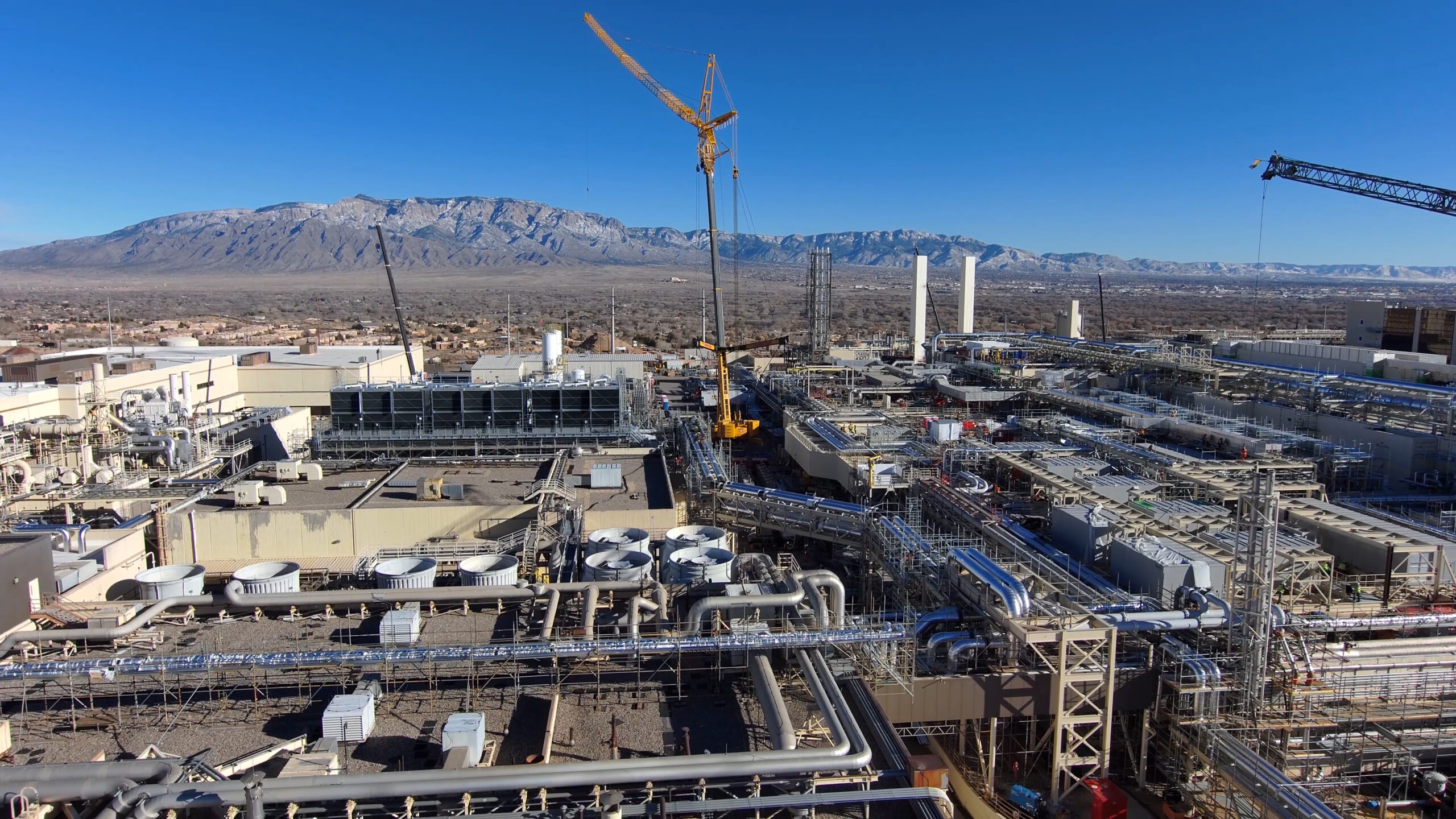
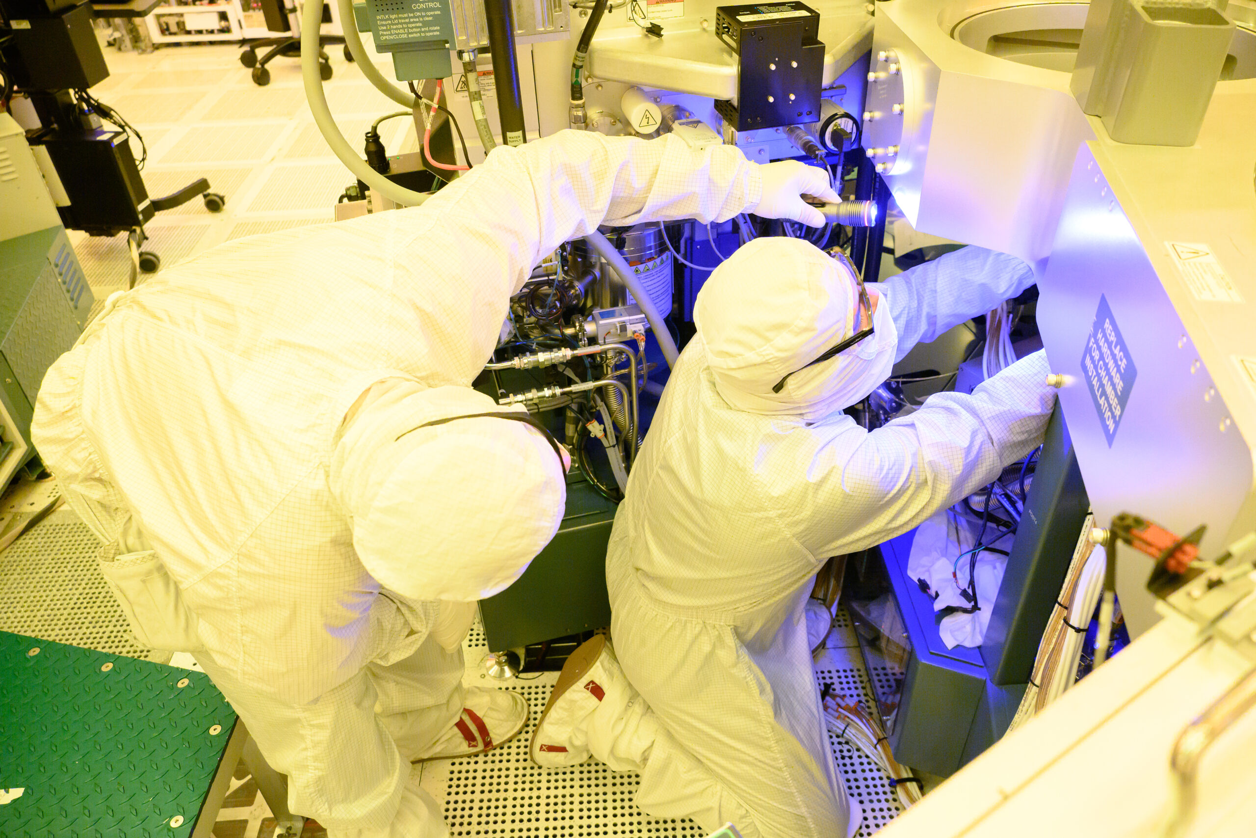
Manufacturing in Arizona, USA
Intel’s Fab 42: A Peek Inside One of the World’s Most Advanced Factories
One of the largest construction projects in the U.S. with almost 6,000 workers is underway on Intel’s Ocotillo campus in Arizona. Intel is outfitting Fab 42 with 1,300 tools (many of them requiring multiple trucks to move), a super overhead highway that zips silicon wafers around all four of the company’s Arizona factories, and a 12-acre water plant that will treat 9.1 million gallons of wastewater a day.
» View video: Intel's Fab 42: A Peek Inside One of the World’s Most Advanced Factories
» View/Download video: Ocotillo, Arizona, Fab 42 Construction (B-Roll)
» View/Download video: Intel Manufacturing Day 2020 from Arizona’s Fab 42 (B-Roll)
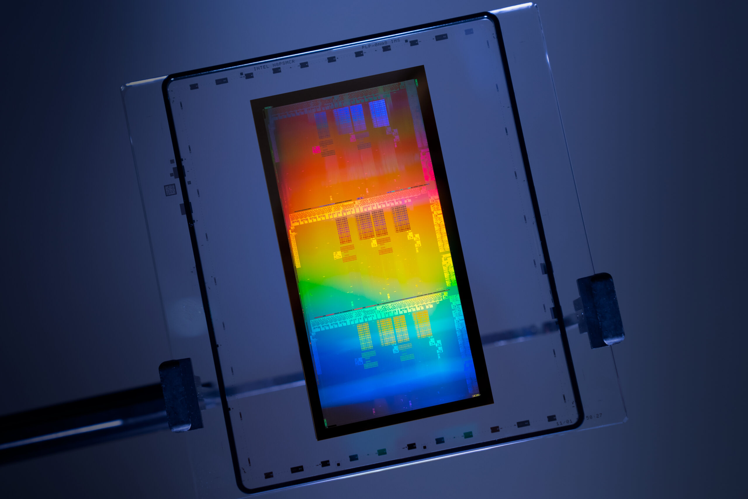
Industry-Leading Glass Substrates

Download all images (ZIP, 50 MB)
Intel Advanced Packaging with Glass Substrates (B-Roll)
Video footage from July 2023 shows glass substrate tools and test units in Intel’s Assembly and Test Technology Development factories in Chandler, Arizona. In the factories, technicians build multi-chip packages that include substrates, computer chips and heat spreaders. Intel is leading the industry with a future generation of substrates made of glass, which will enable power improvements and transistor scaling to continue Moore’s Law. Intel delivers industry-leading packaging breakthroughs that enable performance, cost and scaling benefits for Intel and Intel Foundry Services customers. (Credit: Intel Corporation)
Download video "Intel Advanced Packaging with Glass Substrates (B-Roll)"
Intel’s Masking Operation
Intel Mask Operation: An Inside Look at a Critical Manufacturing Step
Around the corner from Intel’s Santa Clara, California, headquarters is an unassuming building that houses a critically important step in the process of manufacturing chips: the Intel Mask Operation.
What’s a mask? It’s a six-by-six-inch piece of quartz, a quarter-inch thick, that is used as the template to print circuitry onto a silicon wafer. To create a mask, engineers use computerized drawings from chip designers that are the blueprints for Intel processors and their billions of transistors.
Without the Intel Mask Operation, the company’s factories in Oregon, Arizona, Ireland and Israel would be unable to create a single processor. It takes 70 flawless masks to print the many layers of a single Intel 14nm die.
» View video: Intel Mask Operation: An Inside Look at a Critical Manufacturing Step
» View/Download video: The Intel Mask Operation (B-Roll)

» Download all images (ZIP, 7 MB)
Additional Information
Related Posts
Intel and Lens Technology Collaborate to Enable Advanced Semiconductor Packaging for the AI Era
Collaboration combines Intel's advanced packaging expertise with Lens Technology's precision glass processing capabilities to deliver enhanced performance for future AI and datacenter workloads
July 24, 2026

Intel and Fortinet Collaborate to Advance Cybersecurity Innovation and Strengthen Global Supply Chain Resilience
Fortinet’s purpose-built ASIC expertise and Intel’s semiconductor design, packaging, and manufacturing capabilities will drive greater security, scale, performance, and resiliency for organizations
July 21, 2026
