Intel Plans Assembly and Test Facility in Poland

Investment near Wrocław, Poland, will help create a first-of-its-kind end-to-end leading-edge manufacturing semiconductor value chain in Europe.
*** gallery ***
Download all images (ZIP, 53 MB)
NEWS HIGHLIGHTS
- Investment of up to $4.6 billion will create approximately 2,000 Intel jobs and thousands of indirect supplier and temporary construction jobs.
- The new facility will help meet demand for assembly and test capacity anticipated in coming years.
- Facilities will be constructed according to green building principles and will operate with high environmental standards to minimize carbon footprint and environmental impact.
- Intel’s investment will help the European Union work toward its goal of a more resilient semiconductor supply chain.
WROCŁAW, Poland, June 16, 2023 – Intel today announced that it has selected an area near Wrocław, Poland, as the site of a new cutting-edge semiconductor assembly and test facility. This facility will help meet critical demand for assembly and test capacity that Intel anticipates by 2027. Intel expects to invest up to $4.6 billion in the facility, which will have the capacity to expand. When completed, the facility will support approximately 2,000 Intel employees. The construction of the facility is also expected to create several thousand more jobs, in addition to eventual hiring by suppliers. Design and planning for the facility will begin immediately, with construction to commence pending European Commission approval.
Intel’s planned investment in Poland, combined with its existing wafer fabrication facility in Leixlip, Ireland, and its planned wafer fabrication facility in Magdeburg, Germany, will help create a first-of-its-kind end-to-end leading-edge semiconductor manufacturing value chain in Europe. It will also serve as a catalyst for additional ecosystem investments and innovation in Poland and across the European Union.
“Poland is already home to Intel operations and is well positioned to work with Intel sites in Germany and Ireland. It is also very cost-competitive with other manufacturing locations globally and offers a great talent base that we are excited to help to grow,” said Intel CEO Pat Gelsinger. “We’re grateful for the support from Poland as we work to grow the local semiconductor ecosystem and contribute to the EU's goal of creating a more resilient and sustainable semiconductor supply chain.”
Mateusz Morawiecki, prime minister of Poland, said, “We are pleased that the largest greenfield investment in the history of Poland is being led by Intel, a Silicon Valley legend known for its innovation. Chips and semiconductors are critical technologies in the 21st century and we are excited to expand Poland's role in the global semiconductor supply chain and help to establish the country as an economic trendsetter.”
*** image ***
Next Building Block of a Pan-European Semiconductor Ecosystem
Poland was chosen as the location for the new site for several reasons, including its infrastructure, strong talent base and excellent business environment. The new site is also well positioned to work with Intel’s leading-edge wafer fabrication site planned for Germany and its existing leading-edge wafer fabrication site in Ireland. This proximity will enable close collaboration between the three manufacturing sites and help increase resilience and cost efficiency of the European semiconductor supply chain.
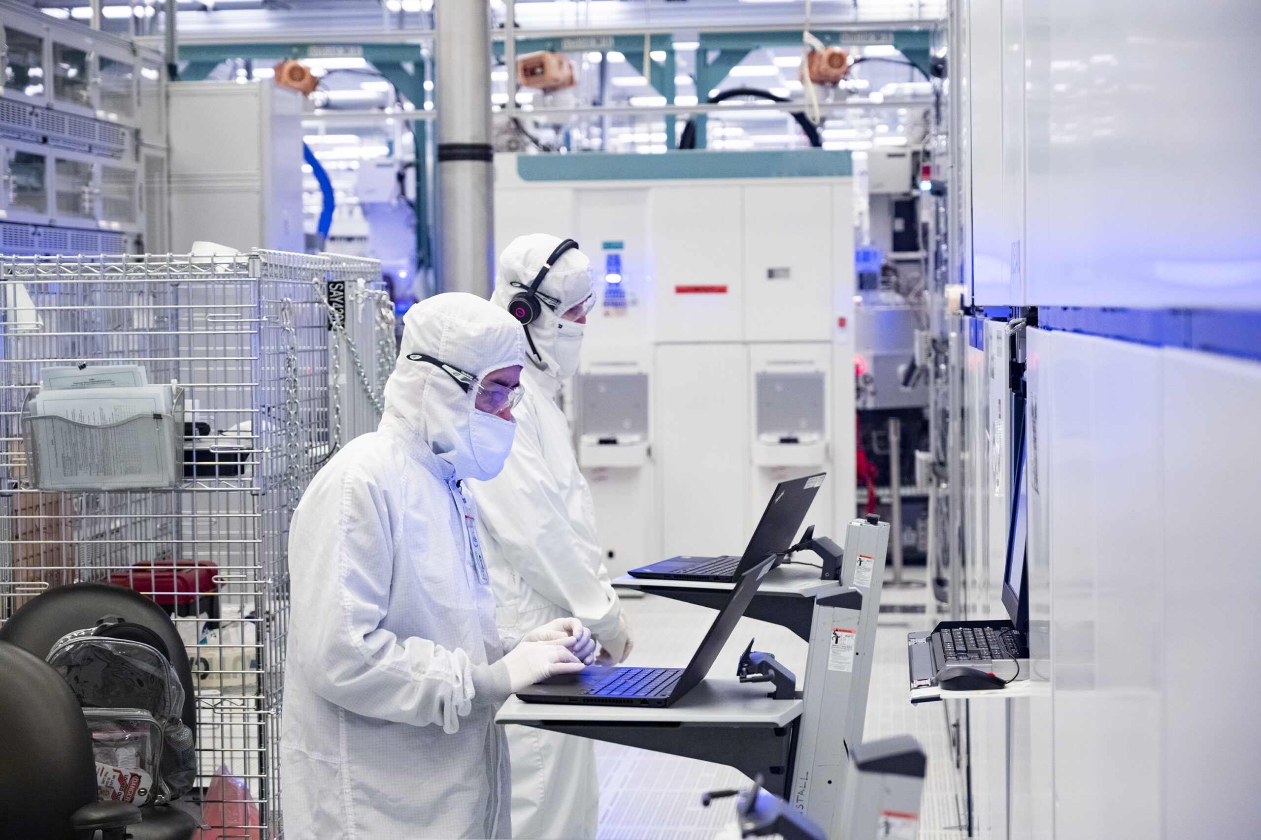
Wafer fabrication facilities (also known as “fabs”) create chips on silicon wafers through various advanced chemical, mechanical and optical processes. Assembly and test facilities, such as the one planned near Wrocław, receive completed wafers from fabs, cut them into individual chips, assemble them into final products and test them for performance and quality. The finished chips are then shipped to customers. In addition to completed wafers, the facility will also be able to accept individual chips and assemble them into final products. The facility will be able to accept wafers and chips from Intel, Intel Foundry Services or other foundries.
The well-paid permanent jobs that the facility creates will range from engineers and business support functions to factory operators and equipment technicians. Poland offers a strong technical talent base and several excellent universities with strong engineering programs. This strong workforce and talent base has been critical to Intel’s 30 years of operation in Poland, including its significant research and development operations in Gdańsk, the company’s largest R&D facility in Europe with nearly 4,000 workers.
A Resilient and Sustainable Semiconductor Supply Chain for Europe
Recent global disruptions show the critical need to build a more resilient supply chain for semiconductors. Intel supports the European Union’s goal to reclaim 20 percent of global semiconductor manufacturing capacity by 2030 and is investing in a global semiconductor supply chain that is resilient and geographically balanced. Intel’s investments in Poland and in Europe can act as a catalyst for further investments by ecosystem companies and for building and attracting the talent needed to support a thriving European semiconductor industry.
Intel is committed to sustainability and will adhere to high environmental standards across its global operations and its European operations, including at the planned facility near Wrocław. This facility will be constructed according to green building principles, minimizing its carbon footprint and the impact on the environment.
Learn more about Intel’s manufacturing technology and worldwide manufacturing operations in Intel’s global manufacturing press kit.
Learn more about Intel’s commitment to sustainability on its Sustainable Computing website on Intel.com.
Forward-Looking Statements
This press release contains forward-looking statements that involve a number of risks and uncertainties. Such statements include: our manufacturing expansion and investment plans and expectations in the European Union (EU) and the anticipated benefits therefrom; anticipated supplier, ecosystem, community, and government support and approval for our planned EU investments and anticipated benefits related to such support; environmental plans for and benefits from our factories and technologies; and other characterizations of future plans, expectations, events, or circumstances.
Such statements involve risks and uncertainties that could cause our actual results to differ materially from those expressed or implied, including: changes in demand for our products; Intel’s failure to realize the anticipated benefits of its strategy, plans, and proposed transactions; construction delays or changes in plans due to business, economic, or other factors; increases in capital requirements and changes in capital investment plans; adverse changes in anticipated government incentives and associated approval related to Intel’s planned EU investments; adverse legislative or other government actions; insufficient ecosystem support; the impact of macroeconomic and geopolitical trends and events; and other risks and uncertainties described in this presentation, our earnings release dated April 27, 2023, our 2022 Annual Report on Form 10-K and our other filings with the SEC.
All information in this press release reflects management’s views as of the date hereof, unless an earlier date is specified. We do not undertake, and expressly disclaims any duty, to update such statements, whether as a result of new information, new developments, or otherwise, except to the extent that disclosure may be required by law.
More: Intel in Poland (Press Kit)
