Device Engineering: Where Ambitions and Real Silicon Collide

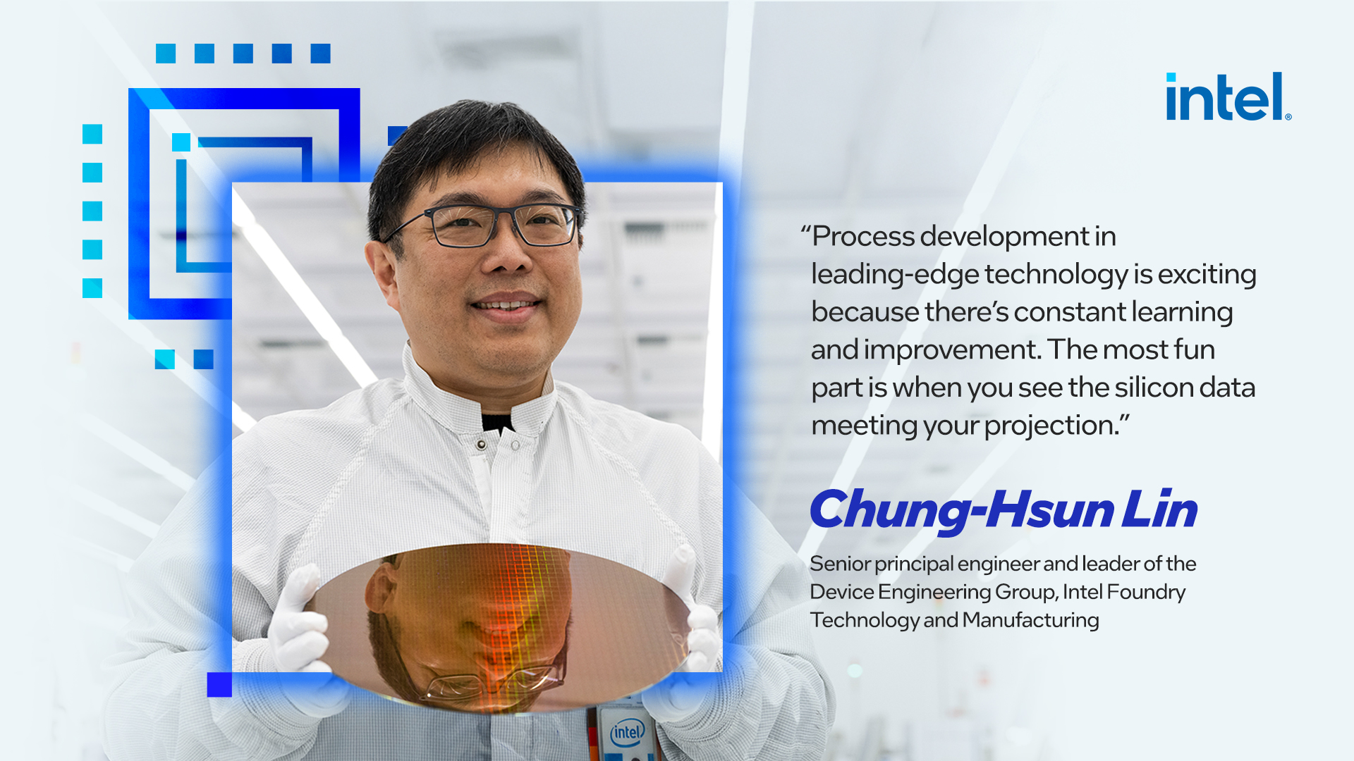
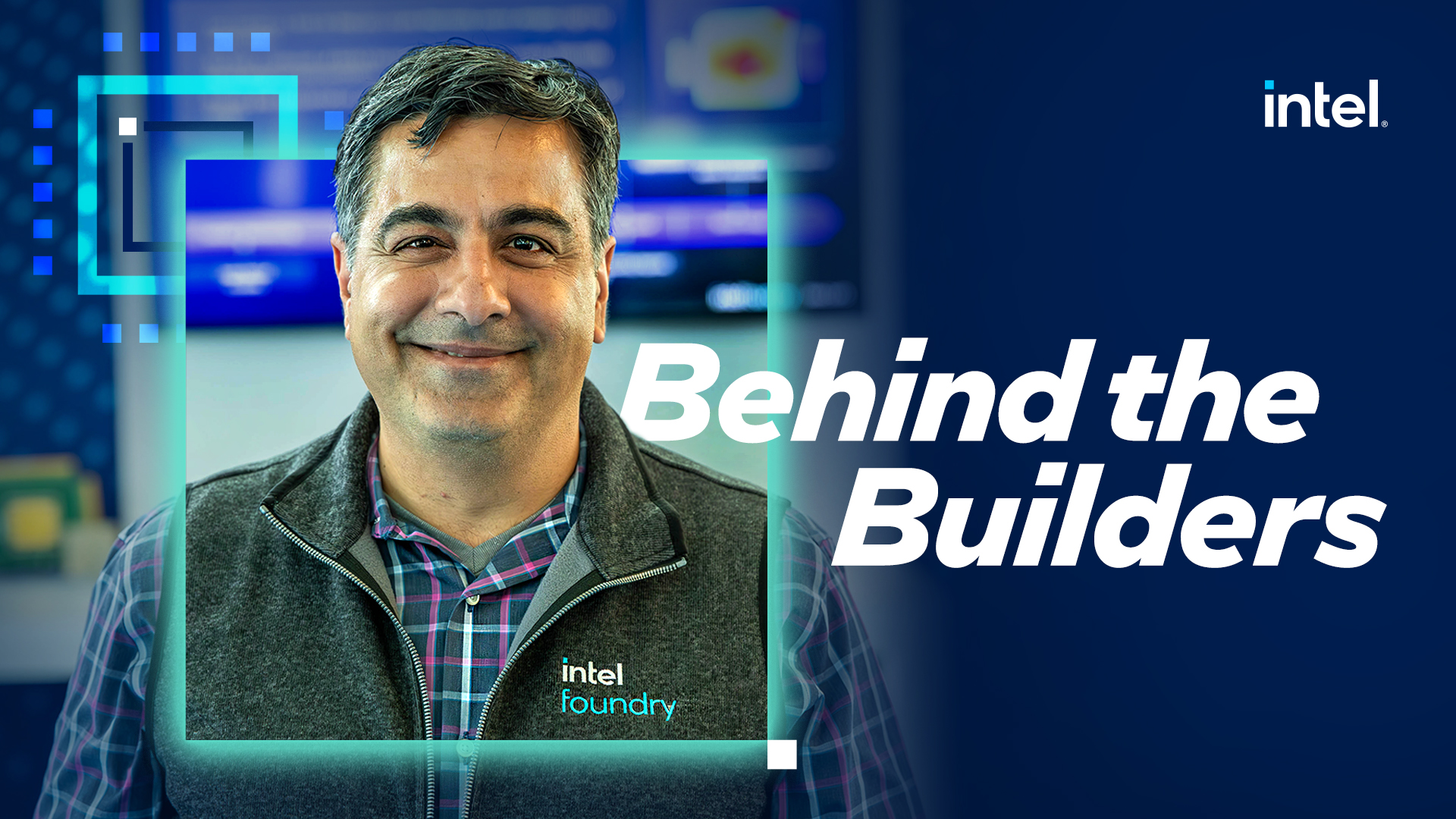
Behind the Builders: As the RibbonFET transistor arrives with Intel 18A, Chung-Hsun Lin works at the crossroads of silicon ambitions and physical reality.
When Global Foundries decided to shift away from the pursuit of leading-edge silicon technology nodes in 2018 (after IBM did in 2015), Chung-Hsun Lin wasn’t ready to give up.
“At that time, I found in my heart, I still want to get my hands dirty working on the leading edge,” Lin says. He had helped build a variety of silicon technologies at Global Foundries and IBM, including the 14-nanometer SOI FinFET process that underpinned IBM’s Summit, which debuted in 2018 as the world’s top supercomputer.
When he joined Intel that same year, he earned a fascinating assignment: leading the pathfinding device group to build Intel’s next-generation transistor, a gate-all-around design later dubbed RibbonFET.
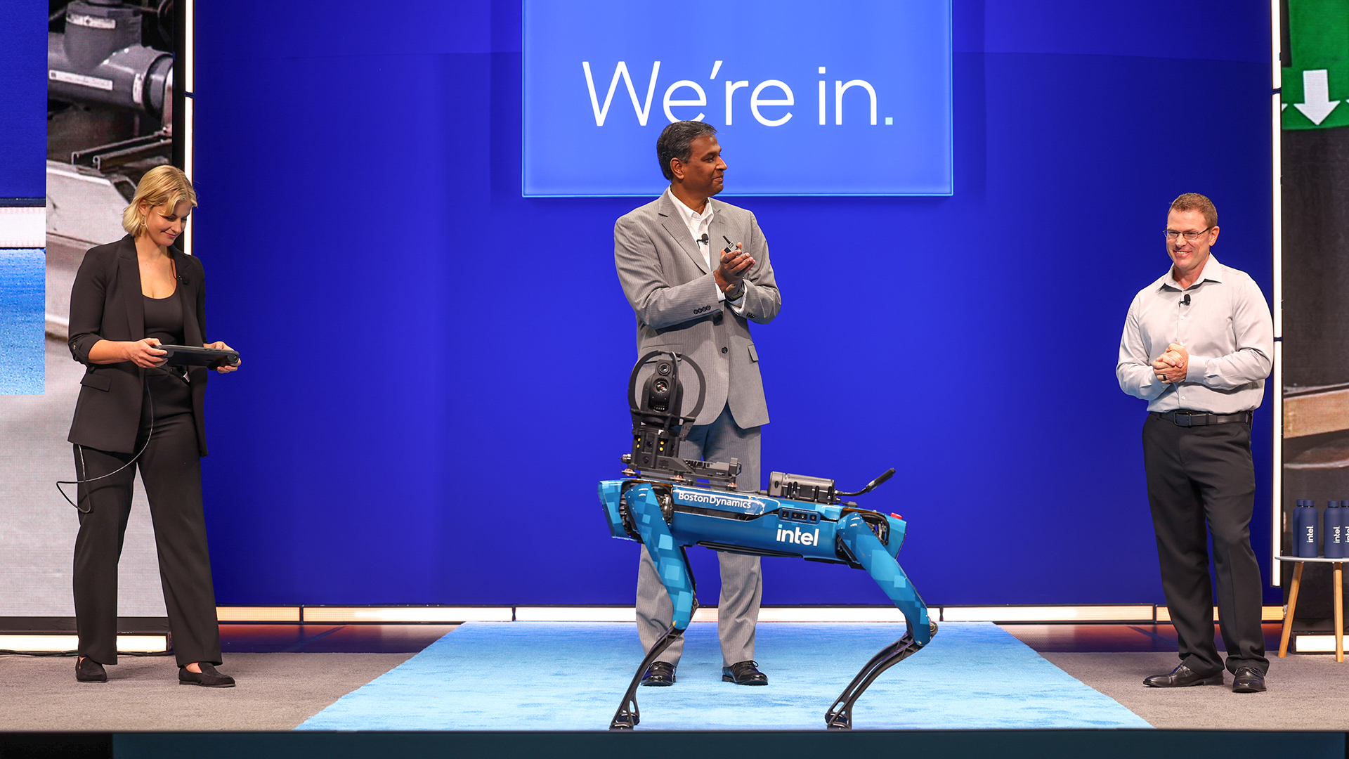
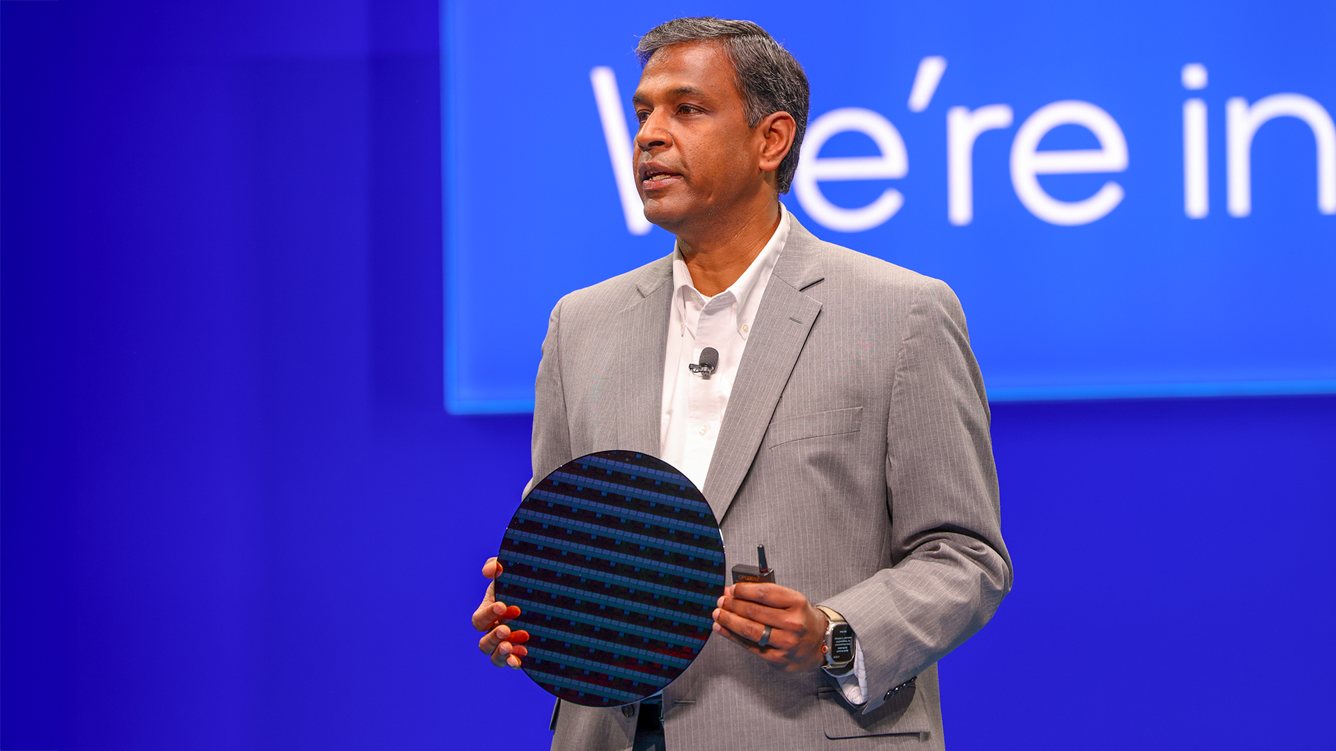
More: All News from Intel Foundry Direct Connect 2025
In 2011, Intel pioneered FinFET, the first major redesign of the CMOS transistor since its 1960s introduction. By the time Lin joined Intel, it was clear another new design would eventually be needed to keep making transistors smaller, faster and more efficient.
If Lin wanted leading edge, he got it. Developing a new transistor would be arguably the most leading-edge job on the planet.
The Intersection of Theory, Silicon Reality and Customer Needs
Almost seven years later, Lin and his colleagues’ toil to turn RibbonFET from concept to high-volume manufacturing has been realized.
RibbonFET makes its debut as part of the Intel 18A process node. Much anticipated for the past four years, Intel 18A is predicted to push Intel back to competitive leading-edge semiconductor manufacturing. It’s the manifestation of Intel’s redoubling on manufacturing prowess and its first major offering as a provider of foundry services for both internal and external chip design teams.
And Lin has played a unique role in its development from his first day at Intel.
Today, Lin is a senior principal engineer and leader of the Device Engineering Group within Intel Foundry Technology and Manufacturing – the division working on several future silicon process nodes, including Intel 18A, Intel 14A and beyond.
Device engineering, it turns out, is where bet-the-company ambitions collide with the reality of what teams can reliably build on silicon wafers. Lin and his team lead a collaborative effort across Intel Foundry to set the performance targets for each future process node – for the transistors and interconnects – and then join forces to achieve those targets in silicon.
They also encapsulate all the resulting specifications for each node in the process development kit, or PDK. “The PDK is how we talk to our customers,” explains Lin. The PDK is no less important than the silicon technologies it represents – he calls it an “implied contract” with customers for how the node will behave and perform.
Owning all this puts device engineering at the center of process node development, reaching deep into both theory and physical silicon processes. “We are kind of a bridge, orchestrating all these things to build the PDK with the process and Design Technology Platform teams,” Lin says. It needs to digitally mirror the physical technologies as accurately as possible.
To complicate things a bit, customers and partners need the PDK early, long before the silicon process is complete and ready for high-volume production. At the beginning, the PDK is the set of years-ahead projections the collective teams think they can achieve by the time process development is complete.
Listening to Customers and Earning their Trust
“We have to be humble,” Lin says. Foundry is all about customer service, “and we are learning to listen to customers and deliver what they need.”
“Process development in leading-edge technology is exciting because there’s constant learning and improvement,” he notes. Customers expect some unpredictability on the silicon frontier, “but they want full transparency.” Embracing collaboration with partners fosters shared insights and, over time, builds trust between internal and external teams.
Lin and team develop and maintain several PDKs in parallel – working to apply lessons across programs quickly and continuously improve the development process itself – but Intel 18A is special. “We’re trying to regain process leadership,” Lin says.
Intel 18A contains a pair of new technologies that are radically different from their predecessors: PowerVia, which moves each chip’s power delivery network to the “back” (the bottom, in layman’s terms) side of the wafer, and RibbonFET, the totally new design for the transistors at the heart of every chip.
Two years ago, Intel proved out PowerVia with a special in-between process node that used well-worn FinFET transistors as a control mechanism to iron out a new two-part manufacturing process, which goes from making chips like pizzas, from the bottom up, to making them like precision flipped omelets.
RibbonFET uses a gate-all-around design and “is probably the most difficult transistor ever built,” Lin says.
Continuing the geometric revolutions, RibbonFET flips the fins of the FinFET on their sides and stacks them vertically, where they can lie as “ribbons” much closer together (from around 30 nanometers apart to 10). It’s worth the trouble: With the gate surrounding the ribbons, the transistors work better. Altogether, each transistor switches faster (delivering more performance), runs more efficiently (using less power) and takes up less area on the wafer. It represents Moore’s Law fulfilled.
What makes the RibbonFET hard to make is its three-dimensional intricacy. To peek into just one slice of it: Materials that form the suspended horizontal ribbons are layered across the entire bare silicon wafer first – and then etched away except where ribbons are needed. New layers are added, trenches are etched, and new materials are deposited in precise locations, sometimes atom by atom.
Triple Trade-Offs, Fulfilling Projections and Unshakeable Optimism
The whole process must be unfailingly repeatable and reliable. “Yield, performance and reliability always hurt each other because whenever you improve one, the other two might suffer,” Lin explains. “They always triple the trade-off.”
But it can be defeated. Lin is a fan of the mindset cultivated by Youssef El-Mansy, a former Intel vice president who led the development of a dozen silicon processes until his retirement in 2004. The recipe, in short: set big goals (like regaining the process lead), take smart risks (see PowerVia’s development), and foster relentless and disciplined execution (hit the schedule).
As development progresses, PDK changes are minimized and the silicon process is refined to match the commitments defined by the PDK. And a lot goes right: “The most fun part is when you see the silicon data meeting your projection,” Lin says.
Last August, Intel Foundry announced that the 1.0 version of the Intel 18A PDK was released, but Lin and team were not done.
Even though the Intel 18A process is entering risk production, Intel Foundry teams continue to improve and expand on its performance and capabilities.
For Lin, the ultimate satisfaction arrives when the technologies reach their destination – in your next laptop or a world-beating supercomputer. “I just want to build something concrete that can help human life,” Lin says.
He knows the next process node, and the next set of challenges, is always right around the corner. For this job, “You need to be a positive thinker and really feel patient about what you are doing,” he says. “You need to be pumped up for many, many years.”
| About Chung-Hsun Lin: Builder in Brief
Home site: Hillsboro, Oregon Title: Senior principal engineer and area manager Team: Device Engineering Group, Logic Technology Development Years at Intel: 6 Management philosophy: “The only way to keep talent is to care about their career growth, define clear engineering goals and empower them to change the world with the resources to do it.” Favorite weekend getaway: Roasting coffee, sipping wine or tea Go-to exercise or entertainment for relaxation: Practicing euphonium and jogging Most-played music on the playlist: Gustav Mahler’s symphonies, conducted by Leonard Bernstein |
Related Posts
How the Science of Burning Buildings Paves the Way to Advances in AI
Behind the Builders: Rajiv Mongia and Intel’s thermal team are pushing boundaries to keep the heat off Moore’s Law and big AI chips that are getting bigger and more powerful.
May 27, 2025

Postcard from Intel Foundry Direct Connect: The Ultimate Factory Tour
A virtual tour through an Intel Foundry semiconductor fab can take you places even technicians and engineers never see.
April 30, 2025