How Silicon Die Become Chip Packages
Intel assembly and test factories put semiconductor chips through brutal tests and finishing touches before they ship.
With the first Tech 101 on semiconductors, you got a high-level overview of how chips are made.
It begins when a bare wafer enters the fab, undergoes thousands of processing steps over several weeks and exits the fab as an astoundingly intricate piece of silicon.
That smart little shard can’t be used in a computer until it completes the second half of manufacturing, called assembly and test. In this process, one or more silicon die are mounted to a “package,” which provides protection from heat and elements, physical strength and connections to the computer.
Welcome to Assembly and Test
At Intel’s assembly and test factories around the world – some with floor space as large as five soccer pitches – technicians complete hundreds of steps to put the finishing touches on each package before it’s shipped to customers.
Here’s an overview of the six major phases each chip undergoes through assembly and test.
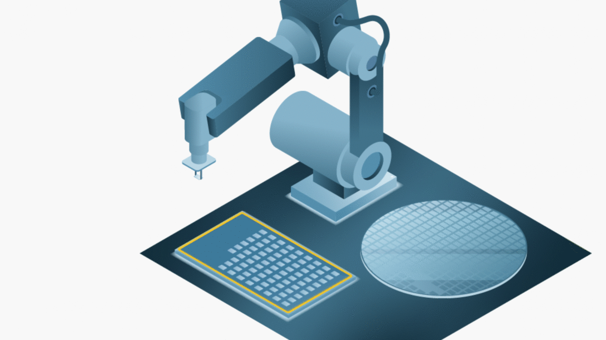
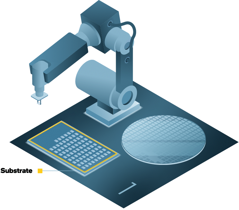
Step 1: Chip Attach
A chip attach module (CAM) affixes die and any other required components (such as capacitors) to the substrate, which is the main body of the package. Substrates are typically organic material, although Intel plans to introduce glass substrates in the near future.
Fun fact: The CAM machine is the size of a car.
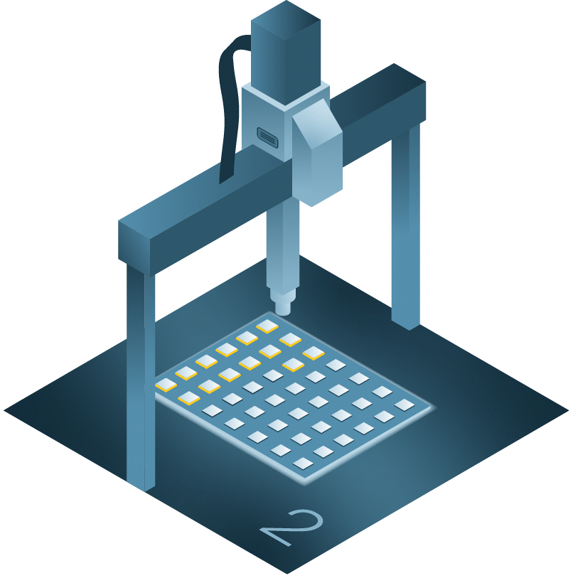
Step 2: Epoxy
Seal it and make it strong: Automated machines dispense epoxy between the die and substrate to remove the most microscopic of air gaps and ensure physical stress is distributed evenly across the die.
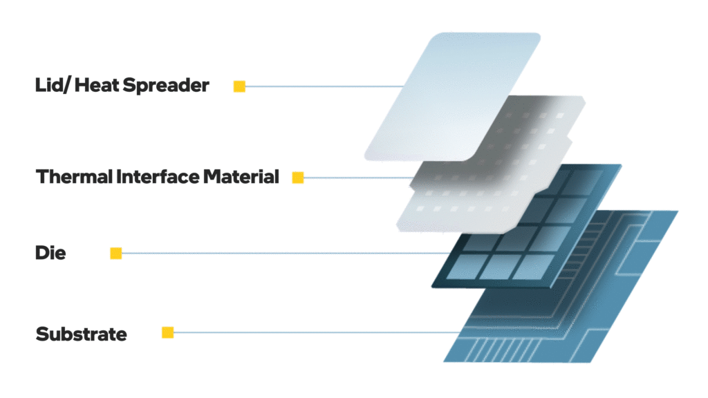
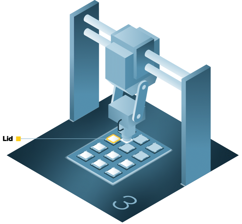
Step 3: Lid Attach
Time for the radiator hat: Machines apply thermal interface material onto the die and then place a heat spreader (known as a lid) on top. The lid helps dissipate heat.
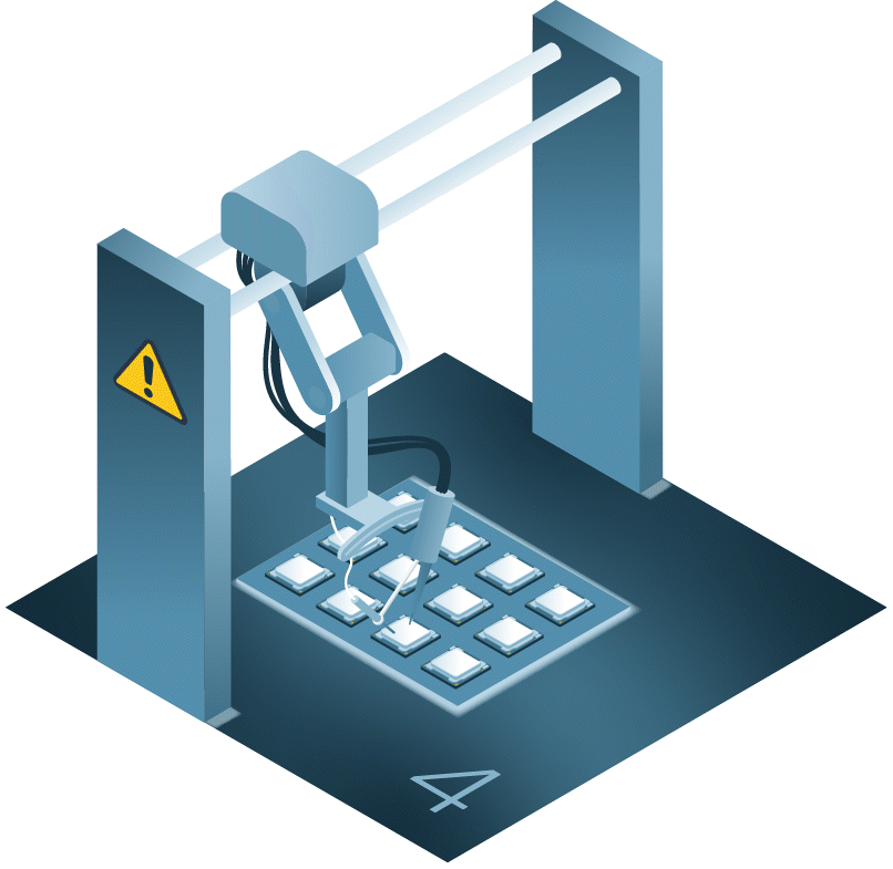
Step 4: Burn In
The pressure cooker: Chips are tested with a heavy dose of high voltage and heat. Only the survivors of this desert proving ground proceed, aimed for a long life of reliability.
Step 5: Test
In the last step before real-world work is applied, each chip undergoes electrical tests to ensure full functionality.
These tests isolate manufacturing defects and track performance to specifications.


Step 6: Process Platform Validation
PPV mimics end-customer conditions by running simulated tests across usage models and operating systems.
Chips that pass all tests are packaged for transport, loaded into trucks and shipped to customers around the globe.
Summary
- The second half of semiconductor manufacturing is called assembly and test.
- One or more silicon die are mounted onto a package, which provides protection and connections.
- Chips undergo a series of electrical, heat and functional tests before they’re shipped to customers.
- Download this Tech 101
Ready to discover more?
The Intel Tech 101 series mixes visuals and descriptions to break down complex subjects and demystify the technology we use every day.
Related Posts

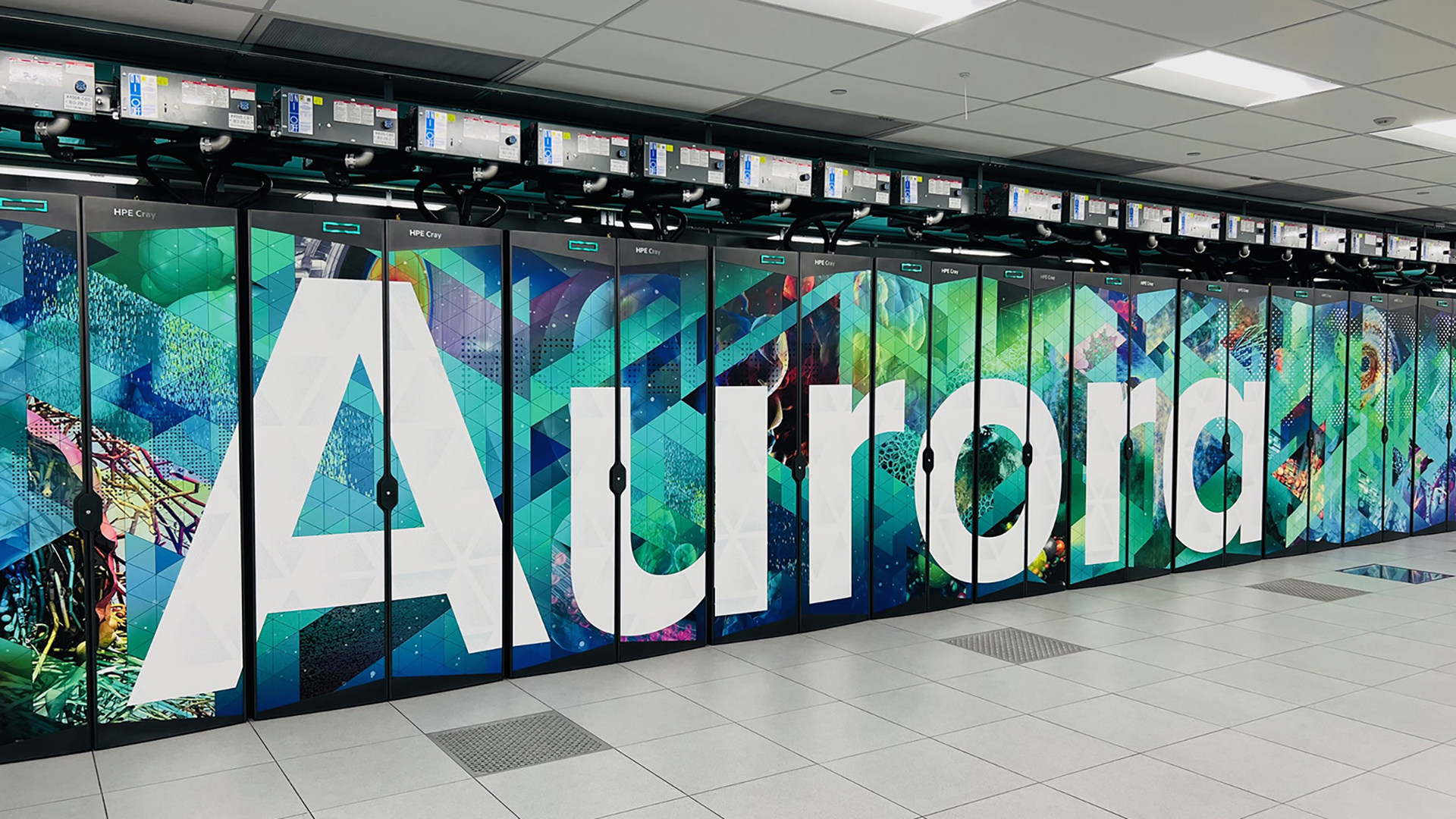
Argonne National Laboratory Celebrates Aurora Exascale Computer
Intel, HPE and DOE leaders and researchers gather to celebrate the collaboration, which is already revolutionizing how scientists use artificial intelligence and simulations.
July 18, 2025
From Circuits to Scale: Intel’s Path to Exascale
As the Aurora Supercomputer reaches its ceremonial opening, three of Intel's team members reflect on the unique scope and challenges of the project.
July 15, 2025