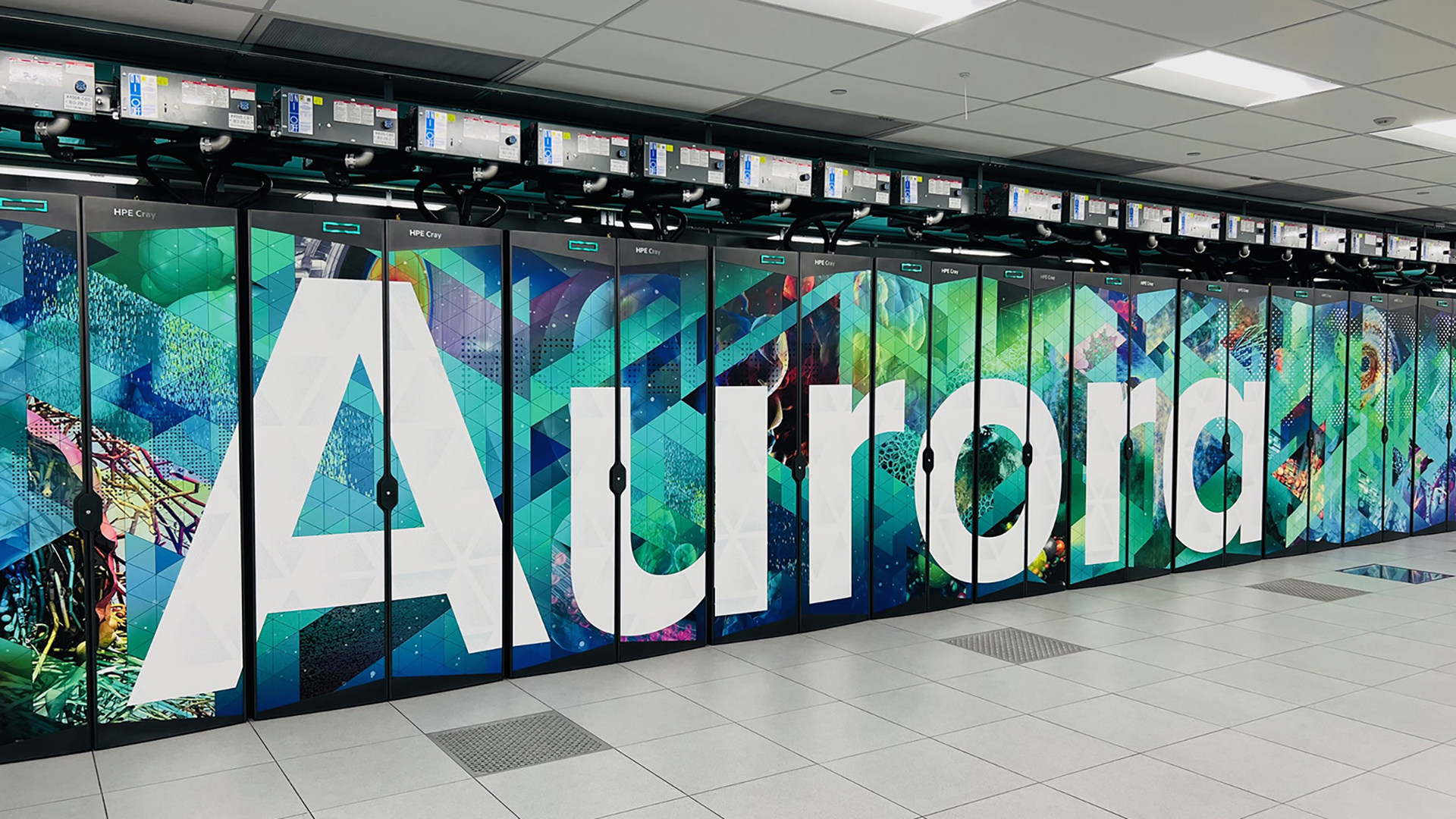
What are Semiconductors?
Semiconductors are the foundation of modern technology. Discover how they work and how they’re made.
Semiconductors work tirelessly behind the scenes to power the world around us – from the technology in your house to the labs curing deadly diseases. They are the foundation of modern technology. Without them, billions of devices across the planet would not function. But what exactly is a semiconductor? And how are they made?
Let’s get right to it. The term semiconductor refers to a material that can be altered to conduct electrical current or block its passage. However, it more commonly refers to an integrated circuit (IC), or computer chip. The most common semiconductor material is silicon. Not surprisingly, silicon is also the main ingredient in computer chips.
How chips are made in the fab

As small as a fingernail, semiconductors are arguably the most complex products ever manufactured. A common chip is only about 1 millimeter thick and contains roughly 30 different layers of components and wires called interconnects that make up its complex circuitry. Billions of microscopic switches called transistors make semiconductors work.
1 Mask operations
Engineers take digital blueprints and convert them into
glass templates, called masks. They are used in fabrication
photolithography, or “printing with light.” As the mask
engineers finish each mask, they send them to fabrication
factories — or fabs — to begin manufacturing.
What are masks?
Masks are templates used to print circuitry onto a silicon
wafer. Mask engineers use computerized drawings from
chip designers as blueprints. Those drawings are fed into
machines that convert the data into an electronic beam
that replicates the circuitry pattern onto 6-by-6- inch
pieces of quartz just a quarter-inch thick. These quartz
squares are called masks. It can tak

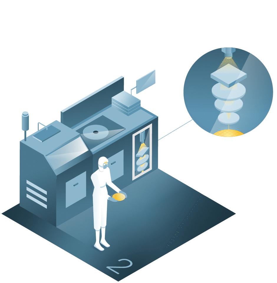
2 Fabrication
Technicians wear bunny suits and use high-tech equipment in
clean rooms to create layers of circuits and devices on silicon
wafers. Each wafer will contain hundreds of chips. From here,
the fab sends the finished wafers to die/sort prep facilities.
What is photolithography?
Silicon wafers are made from the silicon extracted from sand.
Techs use photolithography machines to shine light through
the masks to re-create patterns. A lens reduces the image
and directs it onto a wafer’s surface. This is done repeatedly
using a different mask for each layer of transistors and wire
connections. Eventually the wafer will be imprinted with
hundreds, or even thousands, of tiny individual chips.
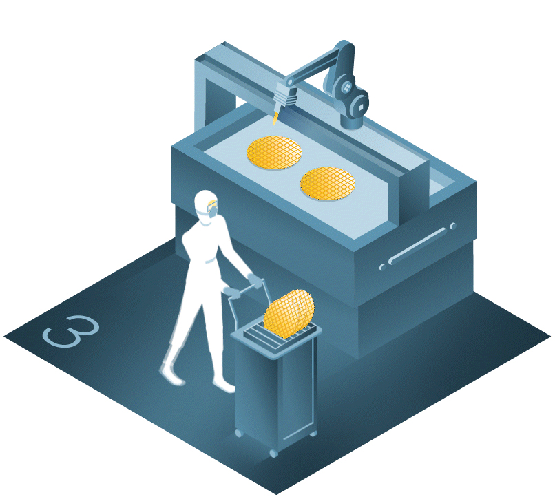
3 Die/sort prep
In these facilities, diamond saws cut the wafers into
thousands of fingernail-size individual rectangles,
each called a die or computer chip. Die and sort prep
machines cherry-pick the working chips and hand
them off to another machine that places them onto
reels. These are sent to assembly and test plants.

4 Assembly and test
Here, technicians take each die and test them one last time to
make sure they’re healthy and good to go. If they pass, they’re
mounted between a heat spreader and a substrate to form a
sleek, enclosed package. The exterior package protects die
from damage, heat and contaminants. Inside a computer, the
package forms electrical connections between the chip and
the circuit board
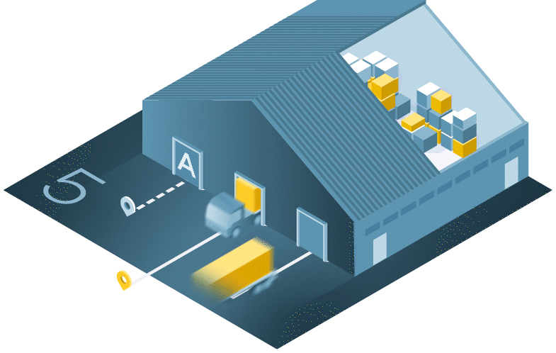
5 Finished goods warehouses/hubs
From here, logistics professionals may send chips directly to
some customers, such as system manufacturers. Or they ship
them to global distribution hubs. From these hubs, chips might
be sent to original eq
Major processor architectures

Field-programmable gate array;
software-configurable circuits
What they do:
Often used in applications that
need to change often, including
acceleration, communications,
circuit design.
Graphics processing unit
What they do:
Make images; accelerate
highly parallel operations.

Central processing unit
(the brain of the computer)
What they do:
Run the computer and all its programs.

Application-specific
integrated circuit
What they do:
One thing very quickly,
including deep learning,
encryption and network
processing.
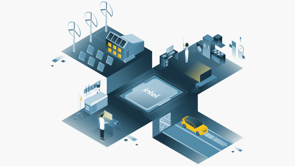
Semiconductors are everywhere
The average American adult spends more than 12 hours a day using electronics, such as computers, mobile devices, TVs and cars. Those devices are all powered by semiconductors, which improve our lives, increase productivity and drive economic growth.
Smart energy
A/C temp sensors
Efficient logistics systems
LED light bulbs
Monitoring systems
Security devices
Smart home systems
Solar panels
Computing
Computers/laptops
XPUs
Diodes
Microcontrollers
RF transmitters
Wireless HD video
Consumer/IoT
ATMs
Smoke detectors
Internet
Refrigerators
Coffee makers
Video games
Washing machines
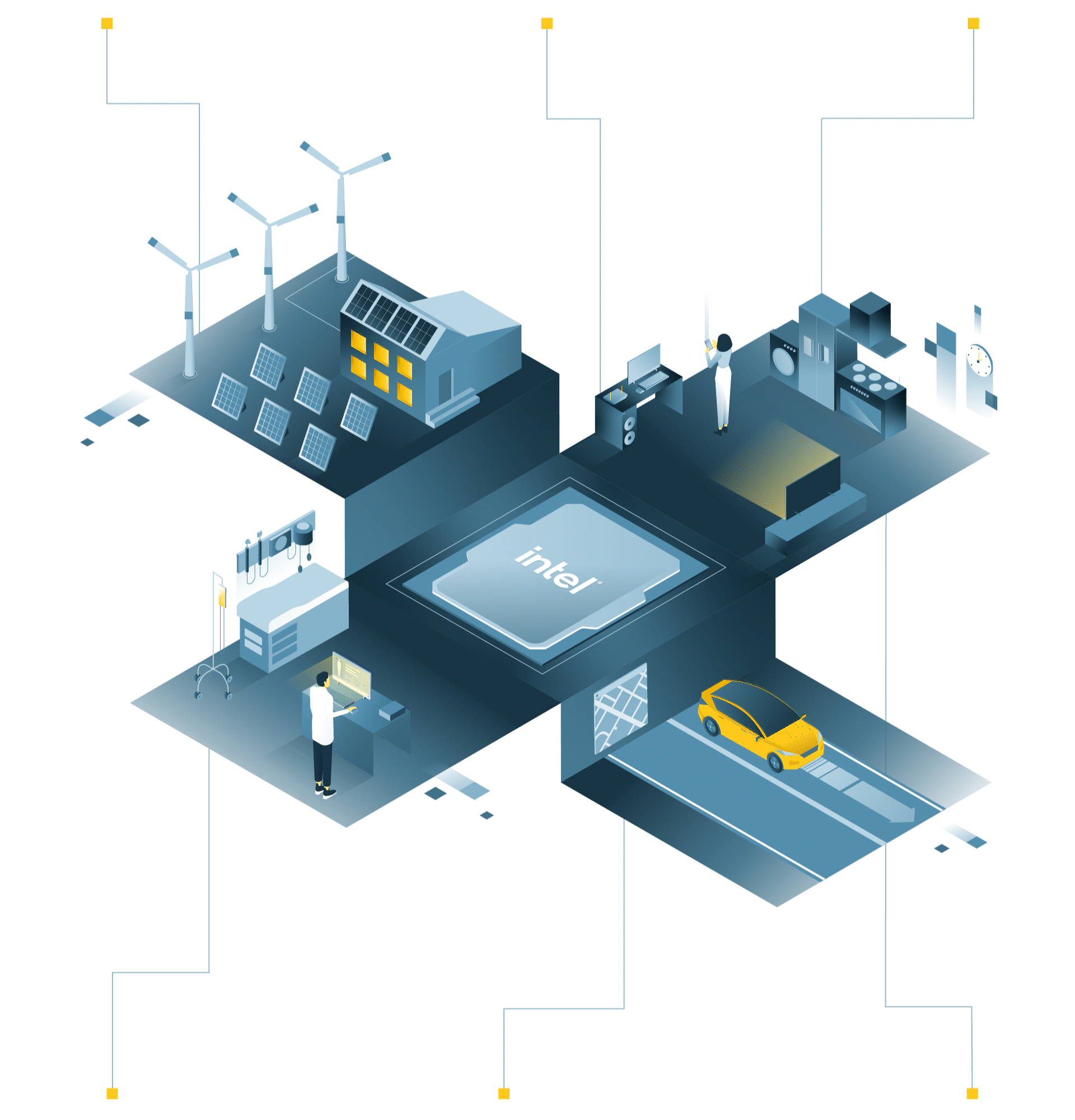
Healthcare
Blood-pressure sensors
Hearing aids
MRIs
Pacemakers
Ultrasound modules
Wireless patient monitors
Transportation
Advanced driver-assistance systems
Diagnostic equipment
Mapping/Sensing
Navigation systems
Communications
Digital cameras
Radios
Scanners
Smartphones
Televisions
Watches/clocks
Intel’s global manufacturing footprint
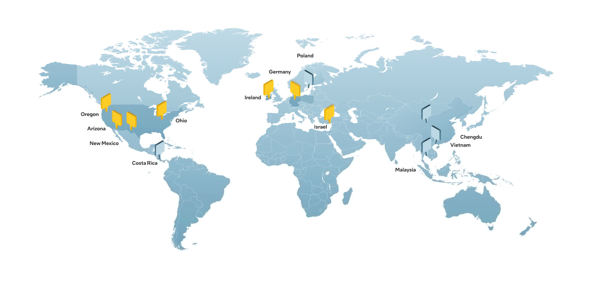
Semiconductors are a worldwide business
$10-15B
The approximate cost to build a new semiconductor factory or “fab”
$574.1B
Global semiconductor industry sales in 2022
12K
The number of construction, high-tech and support jobs a semiconductor fab typically creates
4
American football fields; the equivalent clean room area in one typical semiconductor fab
Summary
- Semiconductors are the foundation of modern technology. They improve our lives, increase productivity and drive economic growth.
- There are many different kinds of semiconductors, each with its own specialty (and acronym).
- Semiconductors are probably the most complex products manufactured in the world. A common chip is only about 1 millimeter thick and contains roughly 30 different layers of components and wires called interconnects that make up its complex circuitry. Billions of microscopic switches called transistors make them work.
- Download this Tech 101
Ready to discover more?
The Intel Tech 101 series mixes visuals and descriptions to break down complex subjects and demystify the technology we use every day.
Related Posts

Intel and Fortinet Collaborate to Advance Cybersecurity Innovation and Strengthen Global Supply Chain Resilience
Fortinet’s purpose-built ASIC expertise and Intel’s semiconductor design, packaging, and manufacturing capabilities will drive greater security, scale, performance, and resiliency for organizations
July 21, 2026
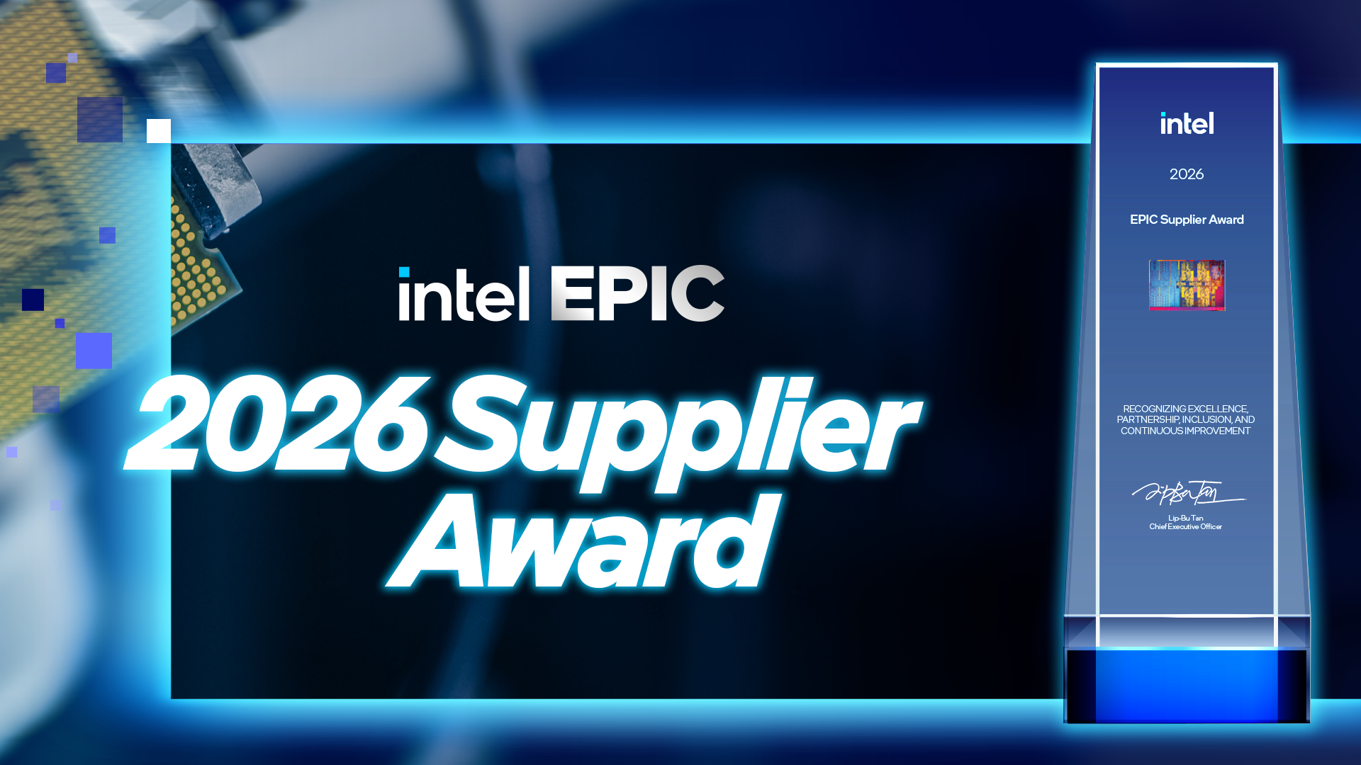
Intel Announces 2026 EPIC Supplier Award Recipients
Annual program recognizes suppliers that exemplify Intel’s standard of excellence.
March 19, 2026